Low Temperature Co-fired Ceramic (LTCC), as an advanced electronic packaging technology, employs a thick-film material system to co-fire electrode materials, substrates, and electronic components in a single process through a pre-designed structure. This technology, with its high integration and superior performance, has become a key pathway for achieving miniaturisation and multifunctionality in electronic systems.
The implementation of LTCC technology primarily encompasses the following three categories:
- Manufacturing of Three-Dimensional Multilayer Circuit Substrates
Low-temperature sintered ceramic powder is formed into green tape with precise thickness and dense structure. Required circuit patterns are constructed on the green tape through processes such as laser drilling, micro-hole slip casting, and precision conductor paste printing. Subsequently, multiple processed green tapes are stacked and sintered at temperatures below 900°C to form chip-scale electronic devices. - Three-dimensional integrated substrates with embedded passive components
Passive components such as resistors and capacitors are directly embedded within the ceramic multilayer structure to construct monolithic three-dimensional ceramic multilayer circuit substrates. This design significantly reduces device volume while enhancing signal transmission efficiency. - Hybrid Integrated Functional Modules
Surface-mounting IC chips and active components onto LTCC substrates creates highly integrated passive/active functional modules. This approach combines LTCC’s high-frequency characteristics with the complex functionality of active devices, making it suitable for applications such as RF front-ends and power amplifiers.
The origins of low-temperature co-firing technology date back to 1982, when Hughes Corporation pioneered low-temperature sintering materials centred on a glass-ceramic system. Through continuous optimisation of material formulations and process conditions, this technology achieved simultaneous co-firing of ceramic substrates and metal wiring layers. Although China’s research in this field commenced relatively late, it has progressed rapidly.
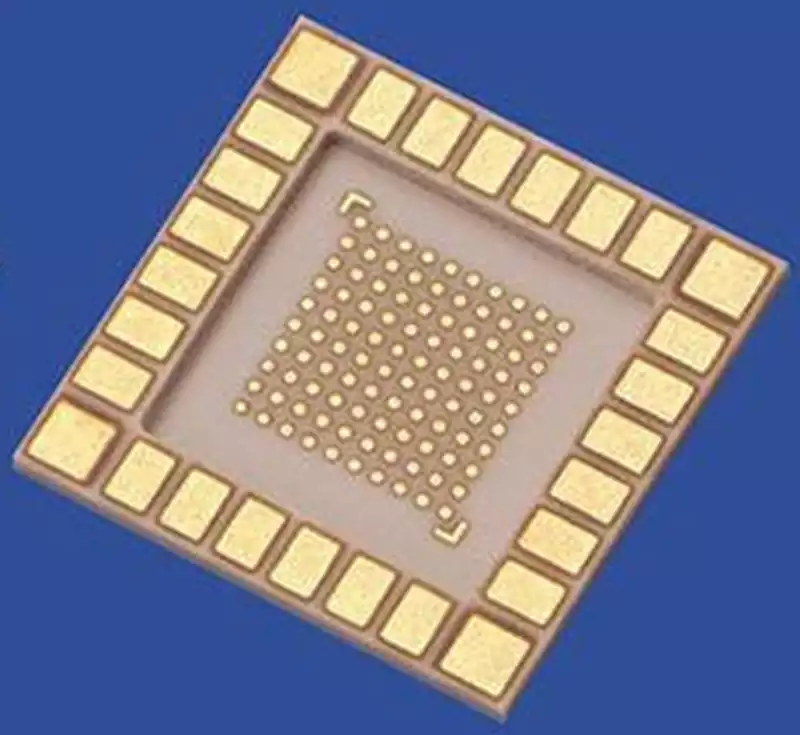
Current global suppliers of LTCC products include international corporations such as IBM, Motorola, Murata Manufacturing, TDK, Rockwell, and Kyocera. Technical reports indicate the industry has produced 50-layer, 16-inch LTCC integrated circuits operating across the 50MHz to 5GHz frequency band. Fujitsu of Japan has successfully developed a 61-layer, 245mm-sized co-fired structure, while IBM in the United States has further advanced this by creating a multi-chip module using a 66-layer LTCC substrate, signifying the technology’s progression towards higher-density integration.
Process Flow in LTCC Technology
① Casting: Forming ceramic substrate blanks from ceramic slurry;
② Cutting: Trimming blanks into ceramic sheets of specified dimensions, each serving as a layer in the multilayer ceramic substrate. Defective sheets are discarded during this process;
③ Punching: Creating vias and through-holes for electrical interconnections via mechanical or laser punching on the sheets;
④ Via Filling: Filling the vias with a via filler material to create vertical pathways for electrical connections between layers, thereby preparing the internal vias of the multilayer ceramic substrate;
⑤ Printing: Using screen printing to deposit conductive paste or dielectric materials onto the ceramic sheets, forming conductive interconnections and printed components (resistors, capacitors, varistors, etc.);
⑥ Lamination: Sequentially stack printed ceramic substrates to align circuit patterns with design specifications, removing the PET film used during printing;
⑦ Static Pressing: Apply high pressure to firmly bond stacked green ceramic substrates;
⑧ Cutting: Separating larger green ceramic substrates along component/module boundaries for subsequent sintering. Post-sintering ceramic sheets become difficult to cut;
⑨ Sintering: Heating green substrates to mature ceramic, hardening the material, curing internal pastes, and stabilising structures. For LTCC substrates, temperatures typically remain below 900°C;
⑩ Resistance Trimming: Fine adjustment of printed components such as resistors to correct printing errors and adapt parameter variations, achieving optimal system performance; ⑪ Testing: Quality monitoring during production prevents defective items from entering subsequent processes. This primarily involves visual inspection, electrical characteristic measurement, and internal structure examination.
LTCC Technology Applications
Multilayer Circuit Integration and Component Innovation
LTCC technology transcends the two-dimensional limitations of conventional circuit boards, constructing three-dimensional circuit structures through the multilayer stacking of green ceramic tape. This design not only supports intricate trace layouts but also enables the direct integration of passive components such as filters, bridges, and antenna radiating elements within the substrate itself. Combined with advanced processes such as thick-film printing, reflow soldering, multi-chip module (MCM) micro-assembly, and metal frame brazing, the LTCC platform achieves high integration of semiconductor bare dies, surface-mount devices, and passive components, ultimately forming fully functional microwave and millimetre-wave component products. Its integrated components encompass a complete range of solutions for substrate-mounted, embedded active/passive elements, establishing itself as the pinnacle of passive integration technology.
Cross-Domain Applications and Market Landscape
LTCC products have expanded into multiple strategic sectors including consumer electronics, automotive electronics, and communications equipment. Within the mobile terminal market, mobile phone applications dominate (approximately 80% market share), followed by Bluetooth modules and WLAN devices. Benefiting from its exceptional reliability, LTCC penetration in automotive electronics continues to rise, establishing it as a core component in in-vehicle communications and radar systems. Typical products include LC filters, duplexers, functional modules, transceiver switches, balun converters, couplers, and common-mode chokes.
Material Innovation and Industrial Breakthroughs
The core competitiveness of LTCC technology stems from the synergistic development of low-temperature co-fired ceramic material systems and processes, where ceramic material properties are the key factor determining product performance ceilings. Currently, the international market offers limited varieties of commercial LTCC green tape, with mainstream materials’ dielectric constants (εr) concentrated within the 5–10 range. These are primarily applied in multilayer substrates, chip inductors, and integrated circuit packaging. To meet diverse product demands, high-dielectric-constant (ε_r > 60) materials have become a research priority. Such materials can significantly reduce the physical dimensions of capacitors and filter units, offering greater design flexibility while enabling the development of high-performance, miniaturised chip filters and antennas.
International giants such as Murata Manufacturing and Taiyo Yuden have established comprehensive material systems. Domestic enterprises, through technological breakthroughs, have broken foreign monopolies, developing supply capabilities for LTCC ceramic materials and配套 electronic pastes covering multiple dielectric constant grades. This material advancement provides a robust foundation for passive integration in 3C products, communication equipment, automotive electronics, and military applications.
Passive Integration Revolution and System-in-Package
LTCC technology enables the in-substrate integration of fundamental passive components—resistors, capacitors, and inductors—alongside complex devices like filters and transformers through three-dimensional wiring. This facilitates the creation of System-in-Package (SiP) solutions when combined with active components such as power MOSFETs, transistors, and IC modules. This technology has become deeply integrated into consumer electronics modules such as mobile phones, Bluetooth, GPS, WLAN, and Wi-Fi, while demonstrating robust growth potential in automotive electronics, aerospace, military communications, micro-electro-mechanical systems (MEMS), and sensors. Its high reliability and space-optimisation capabilities are driving the continuous evolution of electronic systems towards higher integration and superior performance.
From material breakthroughs to system integration, LTCC technology is reshaping the electronics industry landscape through high integration and reliability. It injects innovative momentum into 5G, automotive electronics, and defence sectors, guiding electronic packaging towards a future defined by smaller, faster, and more robust solutions.