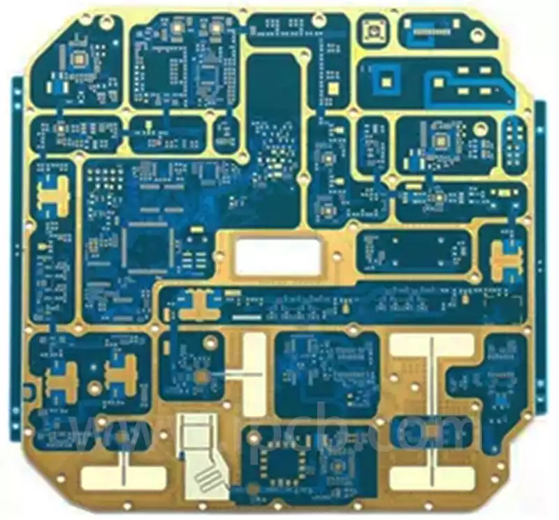
High Density Interconnect (HDI) pcb is widely used in modern high-end electronics due to their excellent performance and compact structural design. However, the manufacturing process of HDI PCBs is complex and involves numerous high-precision technologies and stringent process requirements. In particular, there are many technical difficulties and challenges in the production process, such as microvia production, conductive hole filling, fine line processing, multilayer alignment and material selection.
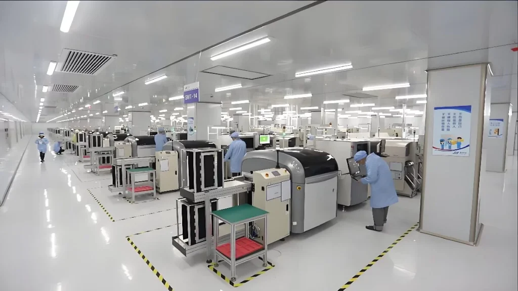
HDI PCB manufacturing process difficulties
1.High technical difficulty in microvia production
Blind vias and buried holes require extremely high production accuracy: in HDI PCB, blind vias are holes that extend from the surface layer to the inner layer but do not penetrate the entire circuit board, while buried holes are located completely inside the circuit board, both of which require high-precision processing technology. Laser drilling is a blind hole and buried holes commonly used in one of the processing means, but the laser drilling equipment investment is expensive, and the laser power, pulse width, frequency and other parameters are very strict control. If the parameters are not properly adjusted, it is easy to cause roughness of the hole wall, uneven hole diameter or damage to the hole wall, which in turn affects the quality and reliability of the over-hole.
Challenges of high-precision mechanical drilling: For larger apertures, mechanical drilling is still used, and the manufacturing of HDI PCBs requires higher precision and stricter tolerance control for mechanical drilling. Factors such as wear and tear on the drill bit, feed rate and RPM during drilling all have a direct impact on the quality of the holes. In addition, due to the HDI PCB layer more and layer alignment requirements, mechanical drilling if there is a deviation or drill jitter, may lead to over-hole position and design deviation, which affects the connectivity of the circuit and the overall performance.
2.Conductive hole filling complexity
Hole wall processing technology requires high: in order to ensure that the conductive material can be firmly filled with holes, the hole wall must be thoroughly cleaned of oil, oxides and other impurities, and roughening to enhance the adhesion of conductive materials and hole wall. However, due to the small size of the HDI PCB board aperture and the depth-to-diameter ratio is large, the hole wall processing is not complete easily lead to conductive material filling is not complete or with the hole wall bonding is not firm, and then in the thermal or mechanical stress under the action of the hole wall peeling, conductive material off and other phenomena, resulting in circuit failures.
The selection and application of filling materials face multiple challenges: filling materials mainly include conductive paste and chemical copper plating two types. Conductive paste filling operation is relatively simple, but its conductivity and reliability is low, prone to drying shrinkage problems, resulting in an increase in the resistance of the over-hole or connection failure. In contrast, the chemical copper plating process can provide better conductivity and reliability, but the process is complex, involving a number of chemical reaction steps, and the process parameters control requirements are extremely strict. For example, the concentration of the solution, temperature, pH and other parameters of the slightest change will affect the uniformity and thickness of the copper plating layer, if not properly controlled, it is easy to uneven plating, copper layer thickness within the hole is not the same problem, ultimately affecting the conductivity of the over-hole and the stability of the connection.
3.High requirements for fine line production
Line width and spacing control is difficult: HDI PCB fine line width and spacing usually reaches dozens of microns or even finer, the production process of photolithography and etching process precision requirements are extremely high. The precision of the photomask in the photolithography process, the resolution of the exposure equipment and the uniformity of the development and etching process and other factors will directly affect the final size and shape of the line. If the line width or spacing is outside the design tolerance, it may cause signal transmission delays, crosstalk and other problems, which in turn affect the circuit performance.
The use of photoresists is challenging: In order to achieve high-precision line fabrication, photoresists must be used. The coating uniformity, exposure and development of the photoresist have a significant impact on the resolution and fineness of the line. In the coating process, if the viscosity of the resist or the coating speed is not properly controlled, it will lead to uneven coating or leakage phenomenon; in the exposure and development stage, changes in exposure energy and fluctuations in the concentration and temperature of the developer may lead to inaccurate pattern transfer, which ultimately affects the accuracy of the line width and spacing.
4.Multi-layer HDI boards require high alignment accuracy
Difficulty of inter-layer alignment: In the manufacture of multilayer HDI boards, the alignment accuracy between the layers directly affects the correctness of the circuit connection and performance stability. Due to the high number of layers and high line density of HDI PCBs, the alignment marks between the layers are easily shifted by pressure, temperature, material shrinkage and other factors during the lamination process. If the alignment between layers is inaccurate, it will lead to misalignment of vias with lines and pads, resulting in serious quality problems such as short circuits or broken circuits.
Alignment equipment and process limitations: Although the current alignment equipment is more accurate, but in the face of ultra-multilayer, ultra-fine HDI PCB manufacturing there are still some limitations. Existing alignment process usually uses mechanical positioning pins or optical alignment system, but in some complex HDI board structure, positioning pin insertion and optical alignment mark recognition may be hindered, thus affecting the alignment accuracy and efficiency.
5.Lamination Process
In the manufacturing process of HDI circuit boards, press-fit is a critical step that directly affects the reliability of the finished product. The pressing process needs to be strictly controlled to ensure uniform thickness and structural stability of the board. For example, in the press-fit process of a four-layer mechanical blind-hole board, it needs to be carried out in steps to avoid board buckling caused by uneven thickness of the board stack.
6.Cost Control
Since the manufacture of HDI circuit boards involves a variety of high-precision technologies and complex processes, such as laser drilling and plating to fill holes, these increase production costs. Especially buried hole technology, its complexity and high precision requirements make the production cost is relatively high, many companies are therefore reluctant to get involved in such processes.
7.Material selection and processing difficulty
HDI board materials compared to ordinary PCB is more complex, usually requires the use of high-performance materials such as PTFE, PPO, PI and so on. These materials have excellent chemical resistance, high strength and high temperature resistance characteristics, but also increases the processing difficulty. During processing, it is easy to produce thermal stress and surface cladding layer rupture and other problems, the quality of the final product.
In the future, the importance of HDI technology will become more and more prominent as the demand for miniaturisation and functional integration of electronic products continues to rise. Manufacturing companies need to continue to invest in research and development to promote the application of new materials, new equipment and new technologies to achieve efficient, stable and cost-controlled HDI PCB production. In this way, they will be able to maintain an edge in the highly competitive market and meet the industry’s growing demand for high-performance circuit boards.