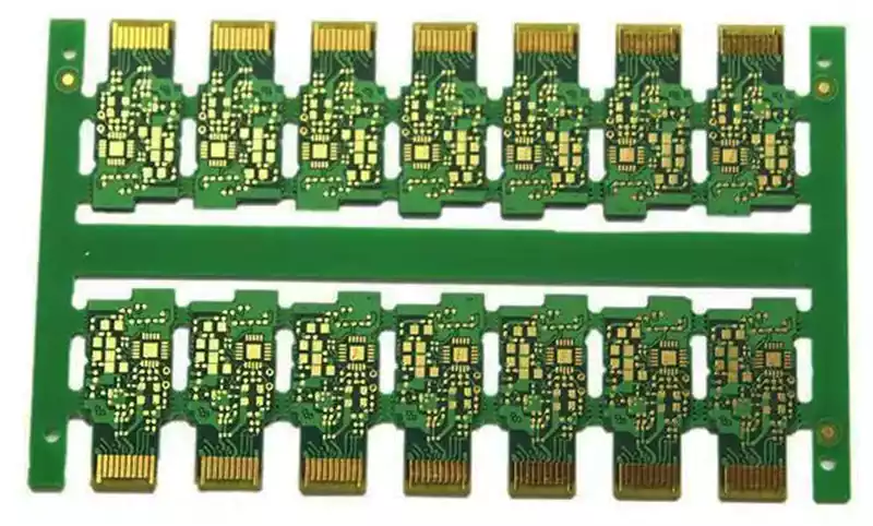
In this era swept by the digital tide, the importance of data centres and communication networks as pivotal hubs for information flow is self-evident. High-frequency optical module pcbs (800G and above), akin to crucial “neurons” within these hubs, shoulder the responsibility of high-speed data transmission, serving as core components that ensure the efficient operation of data centres and communication networks. However, the PCB manufacturing of high-frequency optical modules presents far more formidable technical challenges than their medium-to-low-speed counterparts.
These high frequency PCBs must maintain signal integrity and stability within the ultra-high-frequency band exceeding 100GHz, akin to navigating an extremely narrow and rugged motorway. Any minute fluctuation or interference risks causing a ‘traffic accident’ for the signal, thereby compromising the performance of the entire communication system. Consequently, it imposes near-demanding, extreme requirements on material processing precision, impedance control capabilities, and process stability.
Specialised Processing Techniques for High Frequency PCBs: Fortifying the Foundation of Signal Transmission
The physical properties of high-frequency substrates, akin to the foundations of skyscrapers, directly influence signal transmission quality. iPCB employs a series of specialised processing techniques to comprehensively enhance material stability, laying a robust foundation for stable high-frequency signal transmission.
Substrate Cutting and Storage: Precision Control Ensuring Batch Consistency
During substrate cutting, traditional methods for high-frequency materials like Rogers RO4835 resemble using a blunt knife on precision components, often causing stress concentration at edges that compromises subsequent signal transmission. iPCB abandons conventional methods, employing diamond blades for cutting. With exceptional hardness and sharpness, diamond blades maintain cutting precision within an extremely narrow range of ±0.02mm. This is akin to using an extraordinarily precise surgical scalpel for meticulous cutting of the substrate, ensuring each edge is smooth and flat, thereby eliminating any potential interference with subsequent signal transmission.
Storage conditions are equally critical for substrate performance. iPCB maintains strict storage parameters of 20±1°C temperature and 45±3% RH humidity, with a stipulated storage duration not exceeding 90 days. Under such precise control, the dielectric constant (Dk) deviation for a batch of substrates was significantly reduced from ±0.08 to ±0.04. This ensures each substrate maintains highly consistent performance, akin to a disciplined regiment of soldiers marching in perfect unison, providing a stable and reliable material foundation for subsequent PCB manufacturing.
Surface Roughening Treatment: Enhancing Adhesion, Reducing Interface Reflection
The surface roughness of the substrate significantly impacts copper foil adhesion. An excessively smooth substrate surface causes the copper foil to adhere like a sticker on polished glass, making it prone to detachment. Conversely, an overly rough surface impedes signal transmission. iPCB employs a plasma etching process to roughen the substrate surface, operating at 300W power for 60 seconds. This treatment achieves a surface roughness (Ra) of 0.2–0.3μm, elevating copper foil adhesion to 2.0N/mm—a 30% improvement over conventional chemical roughening methods. This creates a finely textured surface layer, enabling the copper foil to adhere more securely. It effectively prevents signal loss caused by interface reflection during high-frequency transmission, ensuring unimpeded signal passage.
Semi-Cured Sheet Matching: Reducing Laminating Defects, Enhancing PCB Board Quality
The selection and pre-treatment of semi-cured sheets play a critical role in PCB board laminating quality. If the Dk value difference between the semi-cured sheet and substrate is excessive, it resembles joining dissimilar materials, readily creating gaps and stresses that lead to bubbles and voids post-lamination. iPCB employs prepregs with Dk values differing by less than 0.1 from the substrate material, such as Rogers 2929, thereby minimising potential issues stemming from material incompatibility at source. Prior to lamination, the prepreg undergoes a 4-hour pre-bake at 120°C to control volatile content below 0.1%. This series of measures effectively minimises post-lamination voids and bubbles. In the production of an 800G optical module PCB, the lamination void rate was successfully controlled to an exceptionally low level below 0.01%, significantly enhancing the overall quality and reliability of the PCB board.
Precision Control Processes for Impedance and Signal Pathways: Crafting Signal Transmission “Highways”
During high-frequency signal transmission, abrupt impedance changes act like sudden speed bumps on a motorway, causing severe signal reflection and compromising transmission quality. Through multi-stage precision engineering, iPCB ensures meticulous impedance control, forging an unimpeded “highway” for high-frequency signals.
Line Etching Process: High-Precision Forming for Enhanced Circuit Performance
Traditional subtractive etching techniques increasingly fail to meet the precision and performance demands of high frequency PCBs. This is akin to carving intricate patterns with an insufficiently fine chisel, prone to errors and imperfections. iPCB employs an advanced ‘semi-additive process’ to replace conventional methods. This involves first depositing a 5μm thin copper layer onto the substrate, followed by Laser Direct Imaging (LDI) exposure technology. With a resolution as high as 5μm, this technique precisely defines the shape and position of the traces. Subsequent electroplating thickens the copper to a total thickness of 18μm. This process achieves line width precision within ±0.005mm, representing a 60% improvement over subtractive etching. In the production of a 1.6T optical module, differential line impedance deviation was maintained below ±1Ω, providing robust assurance for stable high-frequency signal transmission.
Via Processing Technology: Precision Machining to Reduce Impedance Fluctuations
Vias serve as critical signal transmission pathways within PCB boards, their quality directly impacting signal integrity. Poor via processing, akin to damage in a motorway tunnel, causes signal scattering and loss. Following laser drilling, iPCB employs plasma deburring at 100°C for 30 seconds, achieving a hole wall roughness of Ra ≤ 0.8μm. This significantly reduces signal scattering and loss at via points. Subsequently, a chemical nickel plating (5μm) + electrolytic copper plating (10μm) process is applied, controlling via impedance to 50Ω±2%. This reduces impedance fluctuation by 30% compared to traditional drilling methods. This comprehensive ‘fine polishing’ of the vias ensures signals pass smoothly, minimising reflections caused by impedance mismatch.
Reference Plane Optimisation: Strategic Design for Enhanced Signal Quality
Reference plane design significantly impacts high-frequency signal transmission. Functioning like motorway guardrails, it provides a stable reference for signal propagation. iPCB employs a hybrid ‘mesh + solid’ design for power and ground planes, with mesh line widths set at 0.3mm and spacing at 1mm. This approach ensures effective heat dissipation while maintaining reference plane impedance deviation below 5%. In the production of an 800G optical module, this optimisation reduced signal reflection loss from -20dB to -25dB, significantly enhancing transmission quality and minimising signal degradation and interference during propagation.
Signal Integrity Process Safeguards: Comprehensive Protection to Minimise Signal Loss
High-frequency signals are highly sensitive to path discontinuities, where even the slightest disruption can cause severe signal degradation. iPCB implements a series of process optimisations to comprehensively safeguard signal integrity and reduce transmission losses.
Differential Pair Routing Process: Precise Layout for Signal Synchronisation
Differential pair routing is a common technique in high frequency PCB design, aimed at ensuring synchronous transmission of two signals to minimise interference. Much like two people running together, if their strides are out of sync, they are prone to stumble. iPCB employs a ‘parallel routing + length compensation’ design methodology, strictly controlling differential pair spacing between 0.15–0.2mm (3 times the trace width) and maintaining length differences under 0.15mm. To guarantee routing precision, iPCB utilises AOI’s 3D measurement capability, achieving accuracy of ±0.003mm, with 100% inspection of every PCB. During one production batch, the pass rate for differential pair length difference reached 99.7%, providing reliable assurance for stable high-frequency signal transmission.
Solder Mask Application: Precise Selection to Reduce Transmission Loss
Although the solder mask does not directly participate in signal transmission, its application method and material selection significantly impact transmission loss. Should the solder mask material exhibit high loss characteristics, it would be akin to laying a coarse surface on a motorway, thereby increasing resistance to signal propagation. iPCB employs low-loss solder mask inks with a loss factor Df < 0.003@10GHz, effectively minimising signal attenuation during transmission. Simultaneously, selective coating techniques are employed to bypass differential line areas, controlling film thickness between 10–15μm. Curing temperatures are set at 150°C to prevent high-temperature degradation of substrate properties. These measures reduce transmission loss by 0.2dB/in compared to full-board coating, further enhancing signal efficiency.
Surface Treatment Selection: Premium Processes Ensure Stable Connections
For optical modules exceeding 800G, the selection of surface treatment processes is paramount. This acts as a protective ‘outer layer’ for the PCB board, requiring both aesthetic appeal and durability. iPCB employs a ‘chemical plating palladium-nickel-gold’ process, sequentially depositing a 0.1μm palladium layer, a 5μm nickel layer, and a 0.8μm gold layer onto the PCB board surface. This process not only achieves contact resistance below 10mΩ but also maintains coating integrity without cracking after 1000 thermal shock cycles (-55°C to 125°C), guaranteeing stable high-frequency connector performance. This is akin to equipping the PCB with robust ‘armour’, enabling it to maintain excellent functionality even in harsh environments.
Quality Control System for High-Frequency Processes: Rigorous Oversight Ensures Product Consistency
To guarantee stable and reliable high-frequency PCB manufacturing, iPCB has established comprehensive specialised testing standards. These standards enforce strict quality control across multiple stages, ensuring every PCB board meets premium quality requirements.
High-Frequency Testing: Comprehensive Inspection for Precise Performance Control
Each PCB board undergoes rigorous high-frequency testing post-manufacture. Testing encompasses three-point impedance measurements at 10GHz, 28GHz, and 56GHz, with precision reaching ±0.5Ω, enabling accurate assessment of impedance performance across different frequency bands. Concurrently, insertion loss and return loss testing spans the 1-110GHz spectrum, comprehensively evaluating signal transmission capabilities. During testing of a 1.6T optical module PCB, insertion loss at 56GHz was successfully controlled within 1.2dB/in, ensuring high-quality transmission of high-frequency signals.
Environmental Validation: Simulating Extreme Conditions to Ensure Long-Term Reliability
To validate PCB board reliability during prolonged operation, iPCB conducts randomised thermal cycling tests. PCBs are subjected to 1000 hours of cyclic testing within a -40°C to 85°C environment. This simulates an extended ‘extreme endurance challenge,’ testing the PCB’s tolerance under harsh conditions. Results demonstrate less than 2% change in impedance and less than 0.03 variation in Dk value post-testing, fully meeting the long-term operational requirements for high-frequency modules.
Process Traceability: Comprehensive Documentation Ensures Process Stability
iPCB has established a robust process traceability system, meticulously recording over 300 data points including substrate batches, etching parameters, and test results. Through analysis and monitoring of this data, the CPK (Capability Index) for high-frequency process parameters is maintained above 1.67, guaranteeing process stability and consistency. This is akin to creating a detailed ‘file’ for each PCB board, enabling rapid root cause analysis when issues arise and facilitating timely improvements and optimisations.
The manufacturing of high-frequency optical module PCBs represents a journey of deep integration between precision engineering and high-frequency physical characteristics. Through specialised substrate treatment, precise impedance control, and signal integrity safeguards, iPCB has successfully achieved stable mass production of 800G/1.6T optical modules. These process innovations not only effectively resolve signal loss and reflection issues during high-frequency transmission but also ensure product consistency through rigorous quality control. This provides a reliable hardware foundation for next-generation high-speed communication networks, propelling the rapid advancement of the information age.