As radio-frequency communications, millimetre-wave radar, high-speed interconnects and power modules advance towards higher frequencies, the transmission characteristics of signals within printed circuit boards undergo fundamental changes. Under high-frequency conditions, energy dissipation ceases to be governed by a single dominant factor, instead being determined by the combined effects of material polarisation behaviour, conductor current distribution and structural details. Ceramic circuit board, with their stable dielectric properties and excellent thermal characteristics, have become a vital medium for high-frequency applications. However, their advantages can only be fully realised through systematic treatment of high-frequency losses at every stage of design and manufacturing.
1.Mechanism of High-Frequency Signal Loss Formation
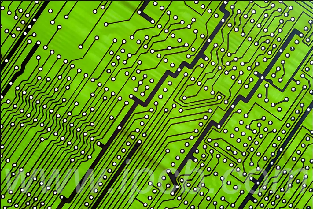
At high frequencies, electrical signals propagate along transmission lines as electromagnetic waves, with their energy continuously attenuating within both the dielectric and conductive layers. Dielectric loss stems from the polarisation hysteresis phenomenon in ceramic materials under alternating electric fields; the faster the field changes, the greater the proportion of energy converted into heat. Concurrently, conductor loss increases significantly with frequency as current concentrates towards the conductor surface, reducing the equivalent conductive cross-sectional area and causing both resistance and thermal dissipation to rise simultaneously.
Beyond inherent material losses, any geometric discontinuities—such as variations in trace width, corners, vias, or interrupted reference grounds—introduce reflections and radiation at high frequencies, further amplifying overall signal attenuation. Thus, high-frequency signal loss fundamentally results from the superposition of material properties and structural response.
2.Fundamental Influence of Ceramic Dielectrics on High-Frequency Loss
The core value of ceramic materials in high-frequency applications lies in the stability of their dielectric properties. Compared to organic substrates, ceramic dielectrics exhibit minimal variation in dielectric constant with frequency and temperature, aiding in maintaining consistent transmission line impedance and thereby reducing reflection loss. Concurrently, ceramic systems with low tangent of loss angle significantly decrease the proportion of energy absorbed within the dielectric.
Different ceramic materials exhibit varying performance at high frequencies. Aluminium oxide is suitable for most microwave applications, while aluminium nitride or composite ceramic systems offer advantages at higher frequencies or in scenarios where loss sensitivity is paramount. Selecting appropriate ceramic materials for specific application bands establishes the foundation for low-loss transmission at the system level.
3.Control of Conductor Losses and Metallisation Structures
At high frequencies, conductor losses may become the primary limiting factor even when dielectric losses are effectively managed. Metal conductors in ceramic circuit boards, typically fabricated using thick-film or thin-film processes, exhibit high-frequency loss levels directly influenced by material conductivity, thickness, and surface condition.
As frequency increases, the skin effect concentrates current near the conductor surface, significantly amplifying the impact of surface roughness on loss. Greater roughness creates more tortuous high-frequency current paths, increasing equivalent resistance. Optimising metallisation processes to reduce surface roughness, while appropriately matching conductor thickness to skin depth, effectively suppresses conductor loss growth.
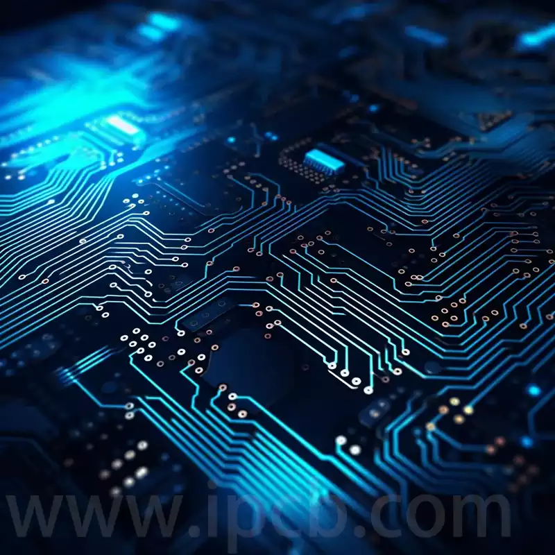
4.Amplification of High-Frequency Losses by Transmission Line Structures
Within ceramic circuit boards, high-frequency signals exhibit extreme sensitivity to transmission line configurations. Transmission lines serve not only as current pathways but also as carriers for electromagnetic field distribution. Structures such as microstrip lines, striplines, or coplanar waveguides require precise design in conjunction with the ceramic dielectric’s permittivity to achieve stable characteristic impedance.
Any abrupt geometric changes disrupt the continuity of electromagnetic field distribution, inducing reflections and additional losses. Consequently, design should minimise sharp bends, sudden width variations, and discontinuous ground planes. For unavoidable interlayer vias, optimising aperture size, pad dimensions, and return paths reduces energy dissipation at vertical interconnections.
5.The Covert Impact of Manufacturing Processes on High-Frequency Losses
High-frequency performance depends not only on the design itself but also heavily on the consistency of manufacturing processes. Insufficient density or micro-porosity defects during ceramic sintering can cause energy scattering and localised absorption within high-frequency electric fields, increasing dielectric loss. Simultaneously, variations in line width, thickness, and edge morphology during metallisation processes can compromise impedance control precision.
Consequently, high-frequency ceramic circuit boards demand far greater process stability than conventional applications. Rigorous control of sintering, metallisation, and post-processing steps, combined with in-line inspection and data analysis, can effectively mitigate the impact of manufacturing variations on high-frequency loss.
6.Collaborative Control of High-Frequency Losses from a System Perspective
In practical applications, high-frequency signal losses are rarely determined by a single factor alone, but rather result from the combined influence of multiple elements. Relying solely on material upgrades or local structural optimisations is unlikely to achieve satisfactory outcomes at the system level.
By incorporating electromagnetic simulation during the design phase to predict losses along critical transmission paths; ensuring manufacturing processes align with design assumptions during production; and continuously refining models through test data during verification, a comprehensive optimisation loop can be established. This systematic approach facilitates a balance between performance, reliability, and cost.
Ceramic circuit boards possess inherent advantages in high-frequency applications, yet controlling high-frequency signal loss constitutes a systematic engineering endeavour spanning materials, design, and manufacturing. Only through meticulous refinement of each stage to address high-frequency characteristics can signal loss be genuinely minimised, thereby unlocking the application potential of ceramic circuit boards within high-frequency, high-reliability electronic systems.