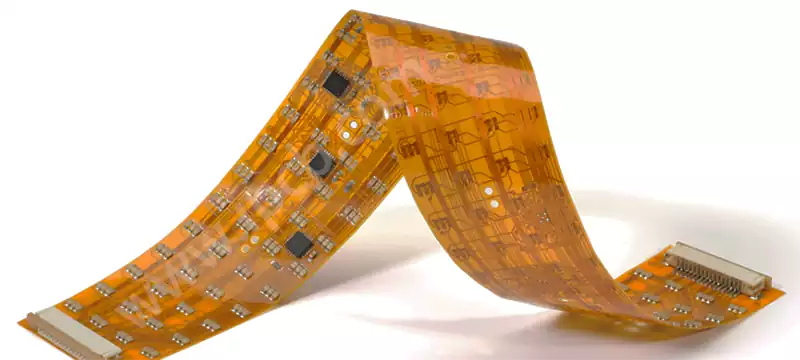
Driven by innovation in consumer electronics, medical devices, aerospace, and other fields, flexible pcb (FPC) have become core components for achieving three-dimensional structural integration and dynamic functionality in devices.
However, the physical properties of flexible substrates differ fundamentally from those of rigid PCBs. Relying solely on the inherent flexibility of the material cannot guarantee long-term reliability under repeated mechanical stress. This paper systematically outlines eight key technical measures to enhance the dynamic adaptability of flexible PCB, covering four dimensions: material selection, structural design, stress control, and manufacturing processes.
Optimization of Multilayer flexible PCB Circuit Structures
- Priority Principle for Electroplated Substrates
For dual-layer and multilayer flexible pcb, replacing rolled annealed copper foil (RA Copper) with electrolytic copper foil (ED Copper) significantly improves dynamic reliability. The columnar grain structure of electrolytic copper foil exhibits superior stress dispersion during repeated bending. Testing demonstrates a 58% reduction in resistance change rate after 100,000 bending cycles compared to rolled copper, making it particularly suitable for foldable display devices requiring high-frequency bending. - Conductor Geometric Parameter Control
Thickness Uniformity: Copper foil thickness variation in bending zones must be controlled within ±3μm. The Semi-Additive Process is recommended for achieving uniform deposition of fine traces.
Width Threshold: Conductor width in dynamic stress zones should be ≥0.2mm. Excessively narrow traces are prone to necking during bending. For 0.1mm trace width designs, replace right-angle turns with curved transition structures.
Layout Design Stress Management
- Bending Prohibited Zone Specifications
Component Prohibited Zone: Within 2mm on either side of the bending axis, no pads, vias, or SMT components shall be placed.
Ceramic Component Safety Distance: Brittle components like multilayer ceramic capacitors (MLCCs) must be ≥3.5mm from the bending edge to prevent microcracks from mechanical stress.
Assembly Warpage Control: Finished flexible PCB warpage must ≤0.7%, achievable by optimizing lamination parameters (pressure 40±5 kgf/cm², temperature 180±5°C). - Trace Routing Optimization Schemes
Orthogonal Trace System: Adjacent layer traces arranged at 90° intersections reduces interlayer coupling stress by up to 35%.
Serpentine Buffer Design: Incorporate U-shaped buffer segments between fixed and free ends, with buffer length ≥ 3 times the bending radius
Minimum Bending Radius: Single-bend radius ≥ 6 times board thickness; repeated-bend radius ≥ 12 times board thickness (e.g., 0.9mm/1.8mm for 0.15mm substrate)
Manufacturing Process Improvement Measures
- Preforming Technology
Cold stamping forming process adopted by professional flexible PCB manufacturers offers significant advantages:
Dimensional accuracy of ±0.03mm, reducing manual forming errors by 90%
Burr-free edges prevent localized stress concentration during use
Enables one-step forming of complex 3D shapes, minimizing material fatigue from repeated bending - Cover Layer Selection Guide
Dynamic Applications: 0.05mm polyimide (PI) cover film, offering 4x higher bend endurance than 0.03mm variants
Static Protection: 0.1mm flexible solder mask layer, must pass IPC-6013 bending test (5mm radius, 100 cycles of 180° bending)
Extreme Environment Applications: Polytetrafluoroethylene (PTFE) cover film, temperature range -200°C to +260°C, friction coefficient as low as 0.12
Special Structural Reinforcement Design
- Notch Stress Relief Solution
When multi-directional bending is required, the following improved structure may be adopted:
Tear-Resistant Hole Design: Reinforcement holes with a diameter ≥0.5mm are placed at the notch end, with an electroplated wall thickness ≥30μm
Wide cut + semi-circular transition: Cut width ≥0.8mm, end semi-circle radius ≥2× cut width
Local reinforcement: Apply 0.3mm-thick polyimide reinforcement sheets or rigid FR4 inserts over cut areas, extending ≥3mm beyond cut edges - Dynamic Fatigue Mitigation Processes
Pre-bending treatment: Pre-bend flexible PCB to 1.5 times the design bending radius prior to assembly to eliminate material processing stresses
Local annealing process: Apply 160°C/3-hour heat treatment to bending zones; grain restructuring enhances fatigue resistance by 60%
Coating Optimization: Replace traditional acrylic coatings with silicone-based elastic coatings, reducing dynamic friction coefficient to 0.1 and wear rate by 75%.
Reliability Verification System
Establish a three-tier testing process:
Material-level testing: DSC analysis confirms glass transition temperature (Tg ≥ 220°C)
Component-level testing: MIT bend test (ASTM D2176) verifies fold resistance (≥ 500,000 cycles)
System-level testing: Real-world condition simulation (including temperature cycling -55°C to +125°C, humidity 95% RH)
Through multidimensional technical optimization and rigorous validation, the dynamic reliability of flexible PCB has been significantly enhanced, now meeting stringent demands such as high-frequency bending and extreme environments. In the future, with continuous breakthroughs in new materials and processes, flexible electronics technology will unlock its potential across more innovative fields, providing more reliable physical carriers for intelligent devices.