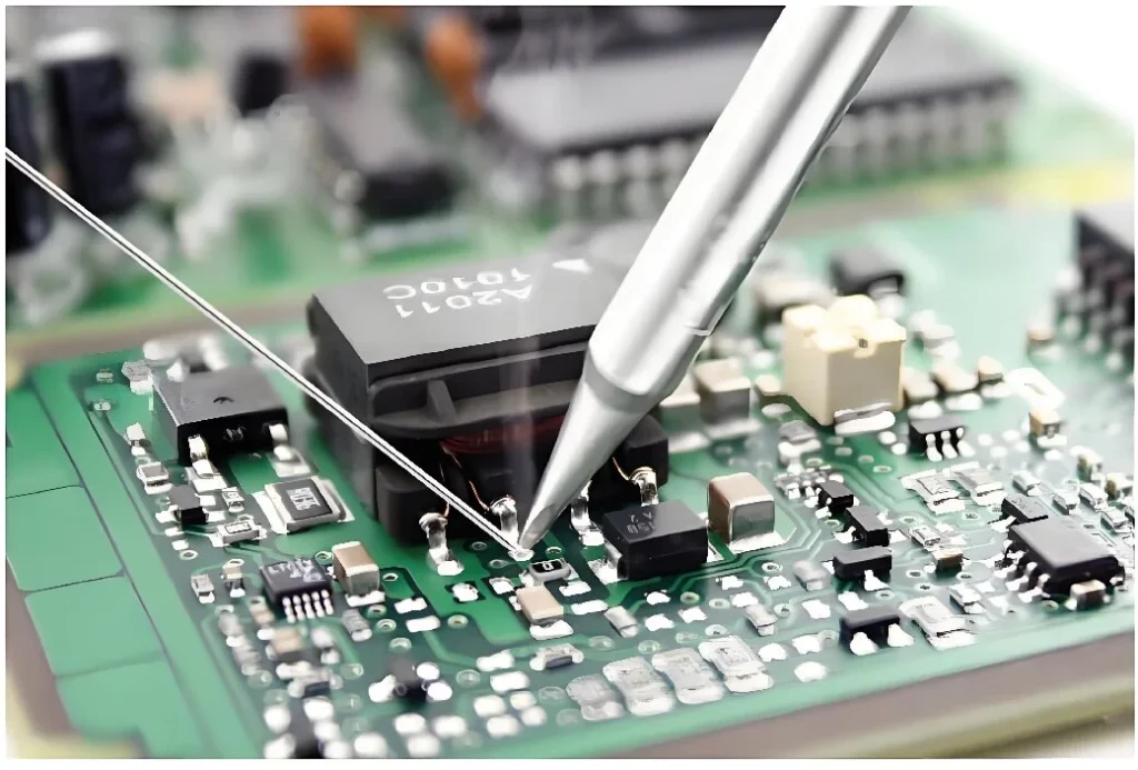
In high-speed optical module packaging, the surface finish applied to the pads of an optical module PCB directly determines wire bonding quality and long-term product reliability. As 100G, 400G, and even 800G optical modules continue to demand longer service life and greater environmental durability, the nickel/palladium/gold (Ni/Pd/Au) three-layer surface finish has become the industry’s preferred solution. This article systematically explains the function of each layer within the Ni/Pd/Au structure and, in conjunction with practical applications in optical module PCBs, discusses its reliability qualification methods and specification standards.
The Nickel Layer as the Primary Diffusion Barrier and Reinforcement Layer
The nickel layer forms the foundation of the entire surface finish structure, serving as both a diffusion barrier and a mechanical reinforcement layer in optical module PCB pad design. Since pad substrates are typically made of copper, whose atoms are highly active, copper readily diffuses toward the surface during high-temperature packaging and long-term operation.
It subsequently reacts with the gold layer to form gold-copper intermetallic compounds. Excessive accumulation of these compounds embrittles the bonding interface, significantly reduces bond strength, and eventually leads to bond lift-off and poor electrical contact.
The dense metallic structure of the nickel layer effectively blocks the upward diffusion of copper atoms, thereby suppressing the excessive formation of harmful intermetallic compounds. Meanwhile, nickel possesses excellent mechanical toughness and structural stability, enhancing the overall mechanical strength of the bonding pads, resisting mechanical stresses generated during packaging, and significantly improving oxidation and corrosion resistance. Without a nickel barrier layer, the copper substrate oxidizes rapidly, causing a substantial reduction in gold wire bond pull strength and severely compromising the long-term reliability required for optoelectronic devices.
The Palladium Layer as an Intermediate Protective Barrier
Located between the nickel and gold layers, the palladium layer serves as a critical transition layer that primarily prevents oxidation and minimizes surface finish failures. When exposed to air, nickel readily reacts with oxygen and moisture to form insulating compounds such as nickel oxide. Once the nickel layer is oxidized, the gold surface can no longer establish a dense metallurgical bond with the underlying nickel, making it difficult to achieve a uniform and reliable gold ball bond. This ultimately results in insufficient bond shear strength, non-wet opens, bond lift-off, and other assembly defects.
Compared with the conventional ENIG process, the additional palladium layer in the Ni/Pd/Au surface finish forms a dense protective barrier that effectively isolates the underlying nickel from oxygen and moisture, preventing nickel oxidation at its source. The palladium layer also eliminates the industry’s well-known “black pad” defect. Traditional ENIG finishes are susceptible to corrosion of the nickel-phosphorus layer, which may result in bond separation, brittle solder joints, and long-term electrical reliability issues.
By providing an additional protective barrier, the palladium layer significantly reduces these risks, greatly improving the operational stability of optical module PCBs in harsh environments and enabling them to successfully pass demanding reliability tests, including 85°C/85% RH temperature-humidity testing, Highly Accelerated Stress Testing (HAST), and salt spray corrosion testing.
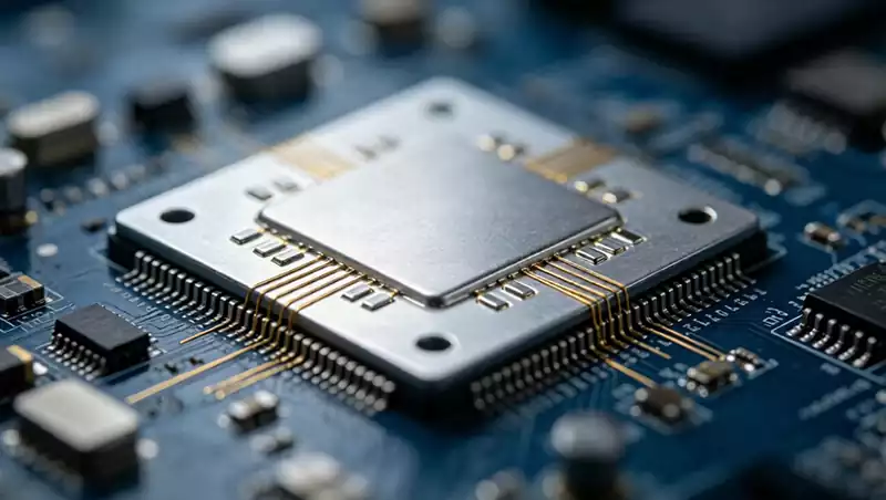
The Gold Layer as the Functional Bonding Surface
As the outermost functional coating, the gold layer provides the direct bonding interface for gold wire bonding, and its quality directly determines wire bonding yield and electrical performance. Gold offers outstanding chemical stability, excellent corrosion resistance, and superior electrical conductivity. It does not form insulating oxide films under either ambient or elevated temperatures, allowing it to rapidly establish a uniform, dense, and low-resistance metallurgical bond with the gold bonding wire. The extremely low contact resistance of the gold layer ensures stable electrical performance during high-speed optical signal transmission while minimizing signal attenuation and interference, making it ideally suited for the high-frequency operating requirements of high-speed optical modules.
However, a thicker gold layer does not necessarily result in better performance. Excessive gold thickness not only significantly increases material costs but also promotes the formation of thicker intermetallic compound layers during wire bonding, reducing interface toughness and increasing brittleness, thereby compromising bond reliability. Consequently, the industry generally adopts an ultra-thin gold finish while maintaining strict thickness control to satisfy bonding requirements.
Why Ni/Pd/Au Is the Preferred Surface Finish for Optical Module PCBs
As the core optoelectronic conversion devices used in data centers, backbone communication networks, and outdoor telecommunications base stations, optical modules demand exceptional service life and environmental durability. Industry standards typically require commercial communication-grade optical modules to operate reliably for 10 to 25 years while withstanding harsh environments characterized by high temperature, high humidity, salt spray, sulfur-containing gases, and repeated thermal cycling.
For optical module PCBs, conventional gold plating alone provides insufficient long-term protection, making the underlying substrate vulnerable to corrosion and eventual bond failure. Although the ENIG process is mature and widely adopted, its corrosion resistance and long-term aging performance are limited, making it less suitable for long-life, high-reliability telecommunications applications. The three-layer Ni/Pd/Au surface finish combines process compatibility, electrical stability, mechanical reliability, and environmental durability through its multilayer protective structure. It provides long-term resistance to a wide range of harsh environmental conditions, ensuring decades of reliable operation and making it the mainstream surface finish for 100G, 400G, and 800G high-speed optical modules.
Corrosion Resistance and Reliability Qualification of Ni/Pd/Au Surface Finishes with Gold Wire Bonding
To verify the reliability of Ni/Pd/Au surface finishes on optical module PCBs, the industry has established a comprehensive qualification system consisting primarily of the following four tests.
High Temperature and High Humidity Aging Test: The standard qualification condition is 85°C at 85% relative humidity for 1,000 hours. After testing, bond pull strength, bond shear strength, and contact resistance are measured to evaluate the moisture and thermal aging resistance of both the surface finish and the wire bonding interface. Qualified products must exhibit no significant degradation in performance and no bond lift-off or structural failure.
Salt Spray Corrosion Test: This test simulates severe coastal and marine operating environments using a continuous 5% sodium chloride solution at 35°C. The evaluation focuses on whether the gold surface develops pinholes or damage and whether the underlying nickel layer becomes exposed or oxidized, thereby verifying the coating’s density and resistance to salt-induced corrosion.
Sulfur Gas Corrosion Test: This evaluation assesses resistance to corrosive gases such as hydrogen sulfide and sulfur dioxide commonly encountered in industrial and outdoor telecommunications environments. Silver bonding wire is highly susceptible to sulfur corrosion, whereas the combination of gold wire bonding and a Ni/Pd/Au surface finish exhibits excellent chemical stability, effectively resisting sulfur-induced corrosion and significantly improving environmental reliability.
Electrochemical Migration Test: Under high-temperature and high-humidity conditions, copper ions from the pad substrate and gold ions from the surface finish may undergo electrochemical migration, resulting in leakage current or even electrical short circuits. The dense Ni/Pd/Au coating effectively blocks ion migration pathways, suppresses electrochemical corrosion, and ensures stable electrical performance throughout the service life of high-speed optical module PCBs.
Standard Specifications for Ni/Pd/Au Surface Finishes and Gold Bonding Wire in High-Speed Optical Modules PCBs
Based on current mass-production practices and reliability requirements, the standard thickness range for Ni/Pd/Au surface finishes used in optoelectronic packaging is 3–7 μm for nickel, 0.05–0.15 μm for palladium, and 0.03–0.10 μm for gold. High-end 100G, 400G, and 800G optical modules generally adopt a tightly controlled configuration consisting of a 5 μm nickel layer, a 0.10 μm palladium layer, and a 0.05 μm gold layer, providing an optimal balance between manufacturing precision and cost.
For carrier-grade optical modules compliant with the Telcordia GR-468 standard, the preferred production specification consists of a nickel thickness of 3–5 μm, a palladium thickness of 0.08–0.15 μm, and a gold thickness of 0.03–0.08 μm. This configuration supports a service life exceeding 20 years while maintaining excellent wire bonding yield, corrosion resistance, and structural reliability.
The diameter of the gold bonding wire used on optical module PCBs should be selected according to operating current, transmission frequency, pad pitch, and chip dimensions. A 0.8 mil (20 μm) gold wire is suitable for low-current, high-frequency applications and is widely used in precision packages such as driver ICs, transimpedance amplifiers (TIAs), and EML laser driver devices. A 1.0 mil (25 μm) gold wire provides the best balance between current-carrying capability and process compatibility, making it the industry’s standard specification for high-volume production. A 1.2 mil (30 μm) gold wire offers greater current-carrying capacity and is specifically intended for high-current, high-power optical modules.
For carrier-grade optical modules, the standard production configuration combines 0.8–1.0 mil gold bonding wire with the optimized Ni/Pd/Au surface finish described above, fully satisfying the core requirements for long-term reliability, manufacturing yield, corrosion resistance, and environmental durability.
The diameter of the gold bonding wire used for wire bonding on optical module PCBs should be selected according to the operating current, transmission frequency, pad pitch, and chip dimensions. For carrier-grade optical modules, the standard configuration combines 0.8–1.0 mil gold bonding wire with the optimized Ni/Pd/Au surface finish thicknesses described above, providing an optimal balance of long-term reliability, manufacturing yield, and environmental durability.