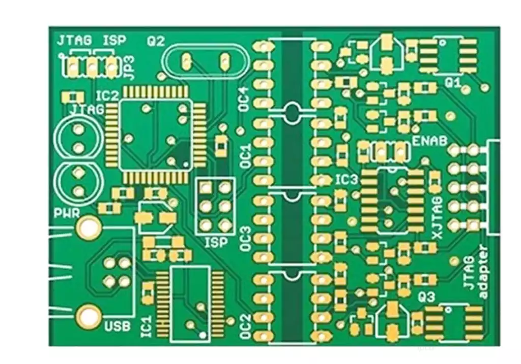
Parasitic means that the capacitance was not originally designed in that place, but since there is always mutual capacitance between the wiring, the mutual capacitance is as if it is parasitic between the wiring, so it is called parasitic capacitance, also known as stray capacitance. Parasitic components are additional components created by the electronics in a circuit and are most often not intended by the design. For example, a resistor is designed to generate impedance, however it actually generates unwanted parasitic capacitance as well.
Parasitic components are inevitable in circuits. All conductors include resistance and inductance, and by duality, such conductors must have capacitance. Component designers cannot completely remove parasitic components, but can only try to minimize their effects.
The most common parasitic components are parasitic resistors and inductors on part pins, and parasitic capacitors on part pin packages. For wire-wound components such as transformers and inductors, the most obvious parasitic effect is the parasitic capacitance between the turns of the winding, which causes the component to resonate at a particular frequency, so that the component is unable to function as an inductor at that frequency (and higher).
Parasitic components are generally represented as lumped circuits, although this may not always be applicable, for example, the parasitic capacitance in the wire-wound component described above is not in a specific location and is better suited to a decentralized component model. Sometimes the component designer can utilize the effects of parasitic elements to achieve a specific function of the component, such as a spiral resonator.
Parasitic elements are also non-linear. Generally non-linear parasitic elements are parasitic structures in integrated circuits due to the presence of a PN junction between two or more electronic components, thus creating electronic characteristics that are not intended at the time of design.
Parasitic capacitance itself is not capacitance, according to the principle of capacitance we can know that capacitance is composed of two polar plates and insulating medium, then parasitic capacitance can not be avoided. For example, a circuit has many wires, the capacitance formed between the wires is called parasitic capacitance. Parasitic capacitance generally in high frequency circuits can have a great impact on the circuit, so the circuit should be specially considered when wiring.
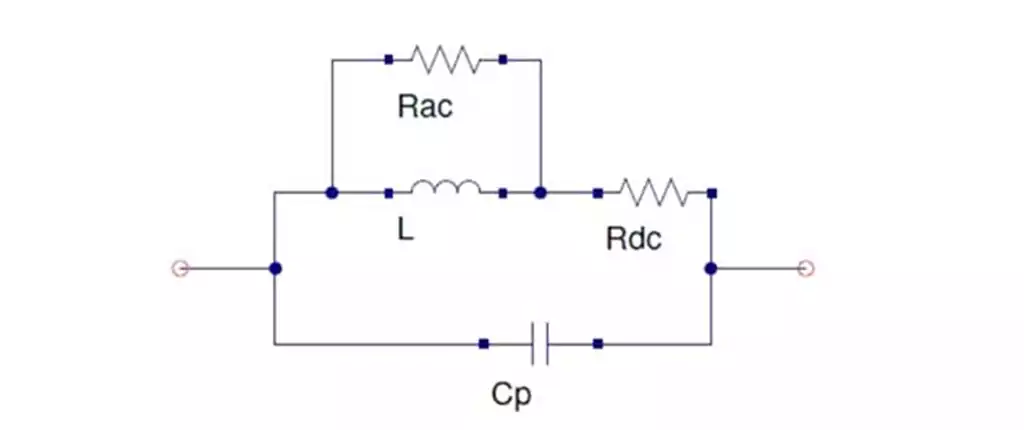
Parasitic capacitance generally refers to the capacitive characteristics of inductors, resistors, chip pins, etc. that are exhibited at high frequencies. In fact, a resistor equivalent to a capacitor, an inductor, and a series of resistors, in the case of low-frequency performance is not very obvious, while in the high-frequency case, the equivalent value will increase, can not be ignored. In the calculation we have to take into account. ESL is the equivalent inductance, ESR is the equivalent resistance. Whether it is resistance, capacitance, inductance, or diodes, transistors, MOS tubes, and ICs, we have to take into account their equivalent capacitance and inductance at high frequencies.
Why does parasitic capacitance arise?
①Insulation layer between pcb components
In circuits, insulation between components is often needed to prevent short-circuiting or leakage, but it also introduces additional capacitance, which affects the performance of the circuit;
② Wires and connectors
Wires and connectors are an important part of a circuit, but they can also generate parasitic capacitance,especially at high frequencies, to the inductive effect of Xi’an and connectors will be more pronounced, thus exacerbating the parasitic capacitance problem;
③ Grounding and power supply
Similarly, grounding and power supply will also introduce parasitic capacitance,grounding and power supply pins and ground or power supply between the insulating layer will form outward capacitance, affecting the performance of the circuit.
Effects of PCB Parasitic Capacitance
Band-limiting behavior in transmission lines, creating low-pass filter behavior at very high frequencies
Noise coupling between different potential grounds, resulting in common mode noise
Noise or signal coupling into components, especially wirewound inductors
High frequency capacitive crosstalk (manifested as FEXT and NEXT)
PDN impedance modification due to spacing between power and ground layers
EMI coupling into the heat sink, generating common mode currents.
How can PCB parasitic capacitance be eliminated?
PCB layout will never completely eliminate parasitic capacitance, but you can reduce parasitic capacitance in PCB layout or take measures to limit its impact on signal and power integrity.
Here is a list of 10 measures you can take to reduce parasitic capacitance on your PCB layout:
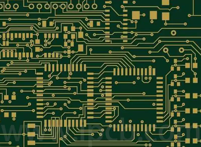
- Avoid parallel wiring
When parallel wiring is used, the area between the metals is the largest and the parasitic capacitance will be the largest. - Remove the power layer
The power layer is usually considered AC ground and is identical to the grounding layer, so removing the power layer is as important as removing the grounding layer near the conductor. - Use a Faraday Shield or Protective Ring
Place a Faraday shield between the two traces to minimize parasitic capacitance effects. - Keep critical traces as narrow and short as possible.
To minimize parasitic capacitance, make critical alignments as narrow as possible so that the PCB process can handle them, keeping a good distance from nearby alignments. - Avoid excessive use of vias
Overuse of vias increases parasitic capacitance. It is best to use patches instead of vias whenever possible. - Avoid component separation
Correct wiring between components, power and ground layers, outputs and inputs, etc. is important to reduce unwanted parasitic capacitance. - The signal layer should be sandwiched between two ground layers or between a ground or power layer.
For example: in a 4-layer board, the power supply layer can be placed on the bottom layer, and in the power supply layer and grounding layer between the wiring of some sensitive alignments, which can prevent the EMI from a layer of signals in another layer of signals caused by noise. - Determine the appropriate layer thickness
Thinner layers reduce loop area and parasitic inductance, but increase parasitic capacitance. - Signal Integrity
Reduced impedance, usually due to proximity to grounded copper lines in the layout
Higher return loss due to impedance mismatch between interconnect and driver/receiver components
Higher insertion loss due to high-pass filtering behavior
The simple solution is to increase the distance between the interconnect and any conductor that is not the desired reference plane.
During design, the width of the alignment on the PCB should be carefully designed to create a coplanar alignment arrangement, taking into account nearby conductors and especially nearby copper cladding.
Copper cladding is a common problem with the signal integrity issues described above.
The PCB Layout should take the time to calculate the minimum clearance required between the copper cladding and its alignment to ensure impedance control. - Power Integrity
Parasitic capacitance can be both desirable and undesirable in terms of power integrity by comparing a PDN structure in a circuit board to one involving multiple grounding systems.
A common situation where parasitic capacitance is undesirable is in systems with multiple grounding points, such as the PCB power ground plane, system ground area, and chassis ground.
In these systems, especially in high-current power supplies, parasitic capacitance can exist between the PCB ground plane and chassis ground, allowing common mode currents to pass through the system and radiate strongly.How parasitic capacitance in the device chassis creates a path for common mode currents when the PCB ground layer and chassis ground have slightly different potentials.
Effective management of parasitic capacitance in PCB design is critical to ensuring circuit performance. With careful layout and routing strategies, we can reduce its negative impact and drive the optimization and development of electronic products.