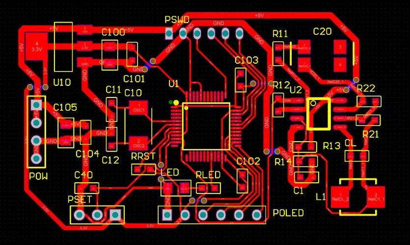
What is a PCB Board Circuit Diagram?
In the field of electronic engineering, PCBs and circuit diagrams are often linked, but they are not simply a matter of drawing a blueprint and a finished product. Rather, they represent a complete system from conceptual construction to physical implementation. A PCB board circuit diagram is essentially an engineering representation used to express electrical connections, component functional logic, and signal flow. It is both the starting point for circuit design and the foundation for the proper functioning of the finished PCB. Whether it’s a simple single-layer board or a high-speed multilayer board with dozens of layers, all layout, routing, layer stack-up, and impedance control must be based on the functional relationships constructed in the circuit diagram. It not only shows how components are interconnected but also describes how current flows, signals are transmitted, power is distributed, and how various functional modules coordinate their operation.
The significance of a circuit diagram goes far beyond simply “drawing a loop.” It transforms abstract electronic principles into concrete, engineering-ready solutions. At this stage, designers must clearly understand the system’s functional requirements, such as the signal processing sequence, power distribution, and control logic structure. Behind every line, node, and symbol in a circuit diagram lies a corresponding real-world electronic behavior, which will be rigorously executed in the subsequent PCB design. If a circuit diagram contains logical errors, missing annotations, or electrical conflicts during the design phase, even a beautifully manufactured PCB may malfunction. Therefore, the completeness and rigor of the circuit diagram are the most critical foundational element in the entire design chain.
Furthermore, circuit diagrams possess deeper engineering value in modern electronics manufacturing. They serve as the blueprint for PCB layout and routing, enabling design software to automatically check interconnect integrity (ERC), component suitability, and signal topology based on node relationships. In complex circuits, such as high-speed differential lines, clock networks, and RF front-ends, the design requires defining the topology, constraint models, and transmission requirements based on the circuit diagram. In short, the circuit diagram not only determines the routing logic but also directly impacts signal integrity, power integrity, and electromagnetic compatibility performance, thereby affecting the overall stability and lifespan of the device.
It is worth emphasizing that the circuit diagram also serves as the communication language for the entire manufacturing chain. R&D engineers rely on circuit diagrams to build product functions; hardware design engineers use them to establish PCB architectures; process engineers use circuit diagrams to identify critical electrical points in production; and quality engineers use them for fault diagnosis and verification. For the supply chain, it serves as the basis for purchasing and verifying materials, and is also a crucial vehicle for suppliers to understand design requirements. Therefore, a complete PCB board circuit diagram is not merely a simple electronic illustration, but a core knowledge asset determining the success of a product.
In today’s highly integrated electronics industry, circuit diagrams are the starting point for all automated design processes. Many modern CAD tools rely on circuit diagrams to perform tasks such as automatic routing, power integrity analysis (PI), signal integrity simulation (SI), and netlist checks. With the increasing prevalence of AI-assisted design, the importance of circuit diagrams has become even more prominent, as they embody system logic and are the foundational data for any automated design decisions.
Therefore, to understand the technical essence of PCBs, one must first understand the engineering value of circuit diagrams. They are not merely drawn, but “designed”; not for display, but to enable a complex system to operate accurately, stably, and efficiently in the physical world.
From Circuit Diagram to PCB Board Design Essence
In the R&D process of electronic products, the relationship between circuit diagrams and PCB boards is often understood as “the former is logic, the latter is implementation.” While this statement is superficially correct, it falls far short of revealing the complex and close connection between the two. To truly understand the design essence of electronic hardware, it is essential to delve into the design philosophy behind circuit diagrams and how they are gradually transformed into a mass-producible, testable, and long-term stable PCB board. This chapter will analyze this journey “from logic to physics” from four perspectives: engineering design process, electrical performance constraints, manufacturing process matching, and system reliability.
In the early stages of R&D, engineers first face abstract functional requirements, such as how a main controller communicates with sensors, how a power circuit supplies power to the entire device, and how an RF module ensures high sensitivity and low noise. These requirements, after analysis and breakdown, are ultimately reflected in the circuit diagram as various electronic symbols, network connections, power supply planning, filter design, and interface definitions. The circuit diagram not only records the functional relationships of the system but also represents a series of trade-offs made by engineers regarding performance, cost, process, and safety. For example, a simple MOSFET driver circuit may seem to have only three or five components, but its driving capability, logic level, current capacity, gate resistance, and reverse absorption capability must all be determined during the circuit diagram stage; otherwise, the entire PCB board will be riddled with problems.
However, a circuit diagram is not the same as a design that can be directly put into production. The circuit diagram focuses on “electrical logic,” while the PCB board’s task is to implement this logic using a fabricable, solderable, and testable physical structure. This conversion process is not a mechanical transfer, but a comprehensive engineering project involving materials engineering, signal integrity, electromagnetic compatibility, thermal management, and factory manufacturability. For example, two signals in the circuit diagram may not interfere with each other, but if improperly routed on the PCB board, they may cause data errors due to crosstalk, or even prevent the device from starting up completely. Or, a filter network in the circuit diagram may be perfect, but if it is too far from the chip on the PCB, the power loop area increases, and the filter network will almost become ineffective.
The first step in converting a circuit diagram to a PCB is to generate a netlist, which is crucial data to ensure that electrical connections are not compromised. However, this step doesn’t mean the circuit logic has been accurately “transferred” to the PCB. Subsequent layer stack-up design, layout, routing, impedance planning, and thermal copper allocation will all re-influence the original electrical characteristics. For example, high-speed differential pairs in the circuit diagram can ensure stable high-speed signal transmission, but in actual PCB implementation, if the differential pairs are not of equal length, do not maintain consistent spacing, or cross segmented reference ground layers, signal integrity will be severely degraded. Therefore, in many high-speed products, a well-drawn circuit diagram is only the foundation; a well-designed PCB board is the key to whether the product can pass testing and certification.
During the layout phase, engineers must extract functional modules from the circuit diagram and place them according to signal sensitivity, power supply noise paths, heat dissipation requirements, and the location of external interfaces. For example, the MCU must be close to the clock source, filter capacitors must be close to power pins, RF modules need to be away from digital switch noise sources, and even the layout orientation of the power supply chip can affect efficiency and stability. Many novice engineers do not consider these physical constraints when drawing circuit diagrams, but experienced engineers will reserve layout space, avoid excessively long loops, pre-define ground reference layers, and plan routing directions. It is evident that circuit diagrams do not exist in isolation, but are inherently interdependent and mutually influential with the PCB board.
The routing phase is crucial for achieving electrical performance. A circuit diagram only tells you how to connect point A to point B, but it doesn’t tell you whether the trace should be shorter, thicker, away from certain areas, whether shielding is needed, whether impedance consistency is required, whether it should be the same length as another trace, or whether there are current return path issues. High-speed signals, RF signals, analog signals, and power networks all require different routing strategies. Engineers must understand the design functionality of the circuit diagram to create the optimal “electrical environment” for it on the PCB board. For example, with a simple ADC input signal, if the trace is routed close to the noise controller area, even with extensive filtering in the circuit diagram, the stability of the final measurement cannot be guaranteed.
On the other hand, modern PCB board design must consider manufacturability (DFM). This directly determines whether the board can be mass-produced and whether the yield meets the company’s requirements. For example, a seemingly harmless inductor in a circuit diagram, if its package is too small, might cause difficulties in surface mount technology (SMT) due to insufficient pad spacing on the PCB. Similarly, a BGA chip with many pins in the circuit diagram, without considering trace density, might require additional HDI structures, increasing costs. In other words, the design of the circuit diagram determines the complexity of the PCB board, and the manufacturability of the PCB board, in turn, requires the circuit diagram to be designed with this in mind from the earliest stages.
At a deeper level, the circuit diagram determines how signals flow on the board, while the PCB determines whether these signals can reach their destination stably, with low noise and low loss. The circuit diagram defines the logical path, but the PCB defines the physical path. The logical path is mathematical, while the physical path carries the real inductance, capacitance, impedance, reflection, loops, and coupling effects. Many circuits work correctly in simulation, but exhibit noise, overheating, and crashes on the actual PCB board because the logical environment differs significantly from the physical environment. Therefore, experienced engineers anticipate potential PCB board issues during the circuit diagram phase and incorporate necessary protection, filtering, isolation, and grounding strategies in advance—a testament to engineering maturity.
In summary, the circuit diagram is the brain of the product, while the PCB board is its body; the circuit diagram determines the system architecture, and the PCB determines its vitality. These are not independent stages but rather a highly intertwined, holistic engineering process. Only by understanding the design purpose behind every line and component in the circuit diagram and constructing the most suitable electromagnetic, thermal, mechanical, and technological environment on the PCB can truly high-quality electronic products be achieved.
PCB Board Stack-up Structure and Material System
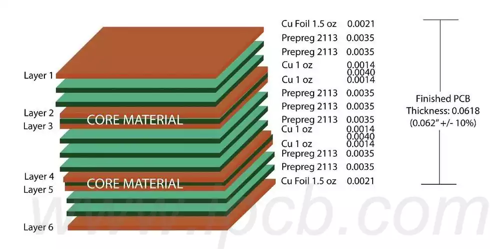
After the circuit diagram completes the logic design, the PCB board enters a crucial stage—the determination of the stack-up structure and material system. Many people believe that stack-up is simply “a few layers of copper foil stacked together,” or “more layers equals high-end,” but this is a very superficial understanding. In reality, the stack-up structure determines signal transmission speed, impedance accuracy, EMC performance, thermal management capabilities, and the overall reliability of the product; it is the fundamental framework of all high-performance electronic products. Almost all electronic devices—from consumer smart devices to industrial control systems, communication equipment, servers, and aerospace vehicles—are heavily influenced by their PCB board stack-up. This chapter delves into this crucial topic to help readers understand why stack-up is the foundation of electronic manufacturing.
In the most basic two-layer board, the stack-up structure seems simple: one side is a signal layer, and the other is a ground or power layer. However, when frequencies rise to tens of megahertz, hundreds of megahertz, or even tens of GHz, and when products need to handle high-speed data, low-noise signals, stable power supplies, and various sensitive modules, two layers are far from sufficient. Signals propagate on copper foil relying on a stable reference plane, and the continuity of this reference plane determines the signal return path. If the stack-up is poorly designed, the return path of high-speed signals is forced to detour, creating a large loop area. This leads to increased radiated noise, worsened crosstalk, signal distortion, and even prevents the device from passing EMC certification. Therefore, in modern electronic design, stack-up is no longer an “option,” but a core element that must be planned in tandem with the circuit diagram.
The first step in layer stack-up design is determining the PCB board’s material system. The most common material is FR4, but FR4 isn’t a single type; it comes in different Tg (glass transition temperature), dielectric constant (Dk), loss factor (Df), and applicable high-speed ranges. Standard FR4 is suitable for most low-speed devices, but when designs scale up to USB 3.0, PCIe, HDMI, 5G communication, radar, or high-speed data acquisition, high-speed materials become indispensable, such as the Panasonic Megtron series, Rogers series, and Taconic series. These materials share characteristics such as lower dielectric loss, higher stability, and smaller dielectric constant deviation, resulting in less signal distortion during propagation on the PCB board. In many products, material selection is even more important than the chip model, because the material determines the fidelity of high-speed signals, while the chip only processes the transmission result.
The second key point in layer stack-up is copper thickness planning. Power layers must be thick enough to carry high currents and reduce voltage drop; signal layers, on the other hand, need to maintain thin copper for precise impedance control. For power boards needing to handle tens of amperes, copper thicknesses can reach 2 oz, 3 oz, or even higher, while layers used for microwave and high-frequency communications may remain thinner at 0.5 oz or less to reduce distributed capacitance. This trade-off must be carefully weighed by design engineers, which is why materials engineering, electrical engineering, and thermal engineering are always interdependent. Many hardware problems, such as overheating, noise, startup failures, and packet loss, are related to inappropriate choices of copper thickness and stack-up.
Besides materials and copper thickness, the layout of power and ground planes is also a critical aspect of stack-up design. Ground planes must be as continuous and intact as possible, avoiding cuts, while power planes need to be partitioned according to different loads to prevent mutual interference. A high-quality ground plane not only serves as a reference but also absorbs noise, improves EMC performance, and provides a stable return path. A rule of thumb is that ground is more important than power; a complete ground plane often improves signal quality more than adding new filtering components. Many beginners place ground planes haphazardly on PCB boards, while true professional design begins with planning the circuit diagram: which signals require dedicated reference layers, which current paths cause interference, and which areas must be isolated.
In complex PCBs with 4, 6, 8, or even more layers, layer stack-up is a complete engineering discipline. For example, in a 6-layer board, a common layout is: signal-ground-signal-power-ground-signal. This arrangement aims to ensure that each signal layer has a complete reference plane during propagation, and that power and ground form a stable “capacitive structure,” thus providing low-noise power to high-speed chips. This layer stack-up structure also reduces EMI, improves immunity, and prevents high-speed signals from easily distorting due to changes in the external environment.
It is worth noting that the layer stack-up structure affects not only electrical performance but also manufacturing costs. The more layers, the higher the cost.The more advanced the materials and the thicker the copper, the more significant the increase in PCB board cost. Therefore, skilled engineers optimize the layer stack design as much as possible while meeting performance requirements. For example, some mid-frequency applications do not require expensive high-speed materials but have high power integrity requirements; in this case, a power plane can be added to the middle layer. Some high-speed interfaces only appear in localized areas; a hybrid lamination structure can be used in those areas to reduce overall cost. This ability to balance performance and cost is an important professional skill for hardware engineers.
Layer stack design also involves an often overlooked but extremely critical element: thermal path design. Modern chips consume significantly more power, especially AI modules, FPGAs, wireless devices, and power conversion modules. Their heat needs to be effectively conducted through copper and dielectric layers. When the layer stack structure is unreasonable, heat cannot flow to the heat dissipation areas, causing the device temperature to rise continuously and eventually fail. By designing heat diffusion layers in the layer stack, increasing copper coverage, and introducing thermal channels in the ground plane, the heat dissipation capacity of the PCB board can be significantly improved. The lifespan and stability of many products actually depend on this hidden structural factor.
In conclusion, the layer stack-up structure is the core element in PCB engineering that best reflects design quality. It’s not simply a matter of stacking layers, but a comprehensive integration of knowledge from multiple fields, including materials, electrical systems, heat dissipation, manufacturing, and reliability. While the circuit diagram determines the logic, the layer stack-up determines the upper limit of product performance; without a reasonable layer stack-up design, even a perfect circuit diagram cannot yield a reliable finished product. It can be said that the layer stack-up structure is the bridge that brings electronic systems from “theory” to the “real world,” and a crucial foundation for every PCB board to become a high-quality product.
Electrical and Manufacturing Logic of Pad and Via Design
In the entire PCB design system of electronic products, pads and vias are often considered the most basic parts, but the simpler the element, the easier it is to hide deep-seated problems. Many circuits perform excellently in simulation but exhibit issues such as cold solder joints, signal jitter, back reflection, enhanced EMI, or even complete board failure in the finished product stage. The root cause is often not insufficient chip performance, but rather that the design of the pads and vias neglected the relationship between manufacturing capabilities, electrical continuity, and thermodynamic behavior. These details determine whether the PCB board can successfully translate the theoretical connections in the circuit diagram into stable physical connections.
Pads are the physical bridge between electronic components and copper foil; therefore, their size, shape, and surrounding solder mask structure must be consistent with the manufacturing process. Designers cannot simply mechanically draw according to the “recommended dimensions” provided by the package library; they must understand that pads inherently bear the effects of solder paste tension, thermal expansion and contraction due to reflow temperature changes, and the influence of stencil misalignment and component tolerances during placement. For example, in small-sized components such as 0201, if the pads are slightly large, the surface tension imbalance during reflow will lead to a severe “tombstone effect”; however, if the pads are too small, insufficient solder paste will result in cold solder joints, contact oxidation, and intermittent poor contact after long-term use. Therefore, pads must find a dynamic balance between process, materials, stencil, and thermal properties. This balance cannot be determined by the drawing alone but requires a thorough understanding of the manufacturing process by the designer.
Via design involves even more complex electrical structures. Many beginners mistake vias for simple “holes,” but in high-speed signal processing, a via is essentially a combination of a miniature inductor and capacitor. With the increasing bandwidth of high-speed interfaces such as PCIe, HDMI, USB4, and 5G RF signals, even a via offset of 0.1 mm can generate reflections sufficient to collapse the signal eye diagram. More importantly, the stub of a via (unused depth) is essentially a short-circuit transmission line that can resonate at certain frequencies, causing electromagnetic energy to accumulate and be reflected within the via. Therefore, high-speed PCBs must minimize stubs, and back-drilling should be used to remove excess copper walls when necessary.
The “combination relationship” between pads and vias is often overlooked by hardware engineers. For example, when routing high-density traces under a BGA, via-in-pad design becomes unavoidable to bring out the traces. However, without resin plugging and smoothing, the solder will be sucked into the holes, causing the BGA solder balls to collapse, or even preventing them from being soldered at all. For high-frequency devices such as RF power amplifiers (PAs), low-noise amplifiers (LNAs), and filters, the number and distribution of vias around the pads, along with the connection method of the ground copper foil, directly affect impedance flatness and parasitic effects. Insufficient ground vias will cause a power drop in the PA; uneven via arrangement will worsen the noise figure of the LNA; and excessively long pad leads or inconsistent distances from the ground plane will significantly shift the passband center frequency of the filter. These phenomena are not apparent in the circuit diagram; they only become apparent under the combined influence of the electrical model and physical structure. Therefore, the copper foil around the pads must be designed in conjunction with the vias to ensure the stability of the RF path.
With advancements in manufacturing processes, via technology is no longer limited to traditional mechanical vias. Laser-drilled microvias are becoming standard, especially in BGAs with pitches below 0.4 mm. Traditional drilling simply cannot achieve fan-out routing, and the advantage of microvias lies not only in their small size but also in their ability to precisely control the connections between signal layers, thereby reducing the impact of vias on impedance and phase. Buried vias and blind vias are also mainstream structures in modern HDI PCBs. They significantly increase wiring density, allowing designers to create more vertical channels within limited planar space. When using a mix of vias, the layer stack-up plan must be determined in advance; otherwise, manufacturing may be impossible due to conflicts in the lamination sequence.
The solder mask layer has a profound impact on pads. The choice between NSMD and SMD pads is not simply a style choice, but rather part of electrical behavior. For example, NSMD pads, due to their more complete copper exposure, can achieve a more uniform solder paste amount, suitable for most devices; however, in BGA or high-current pads, SMD structures offer better mechanical strength and reduce solder joint cracking under thermal shock. For high-speed interfaces, since each pad forms a local capacitance, excessively large pads can change the differential line impedance, leading to mismatches, especially for DDR and PCIe interfaces. Improper solder mask openings can also result in insufficient pad spacing, causing solder bridging and affecting manufacturing yield.
Thermal management is also closely related to pad and via design. For high-power devices (such as MOSFETs, DC-DC modules, GaN, and silicon carbide power devices), the pads must be tightly integrated with the bottom copper layer, a large internal ground plane, and numerous thermal vias to form an effective heat dissipation path. Only by rapidly conducting heat from the bottom of the device to the multi-layer copper foil and then dissipating it can the product maintain stable operation under high loads. Many switching power supply boards experience thermal runaway in experiments, often not due to incorrect thermal simulations, but rather to insufficient number of thermal vias, uneven distribution, small via diameters, or failure to securely connect to the large ground plane.
In summary, pads and vias are not merely “details” on a circuit board, but rather one of the most fundamental structural elements of electronic design. They play a combined role in mechanical, thermal, and electrical aspects, serving as the crucial link between the circuit diagram and the real world. Proper design ensures long-term product stability, strong soldering, signal integrity, and excellent EMI; improper design can easily ruin an otherwise excellent circuit design. Whether a product is for high-speed communication or low-speed control, a high-power module or a light-load device, pads and vias are always the foundation of PCB board reliability and a key technical focus that every hardware engineer must repeatedly consider.
Summary
No matter how complex the architecture of an electronic system is, it must ultimately be translated into functional physical connections through a physical PCB board. The circuit diagram is the idea, the PCB is the reality; the distance between the two may seem like just a change from two-dimensional symbols to multiple layers of copper foil, but what truly determines the success or failure of a product is whether the designer can understand the hidden coupling relationships between electrical, material, thermal, and manufacturing aspects. In high-speed environments, the impedance control of a trace, the shape and location of a via, the size of a pad, and its surrounding structure can all affect system stability; in power circuits, copper thickness, heat dissipation paths, and via arrays directly determine device lifespan; and in signal chains, loop area, ground structure, and reference planes are key factors affecting EMI/EMC.
As electronic products continue to evolve towards higher frequencies, smaller sizes, and higher reliability, PCB design is no longer just mechanical drawing; it has become a comprehensive engineering endeavor spanning materials engineering, electromagnetic theory, thermal management, and manufacturing processes. In actual production, every layer stack design, every choice of dielectric material, and every determination of solder mask openings or via structures must balance manufacturability and performance. If circuit diagrams are the “language” written by electronic engineers, then PCBs are the “industrial works” that translate that language into reality.
Therefore, an excellent PCB is never merely a display of stacked copper layers or routing techniques, but rather the crystallization of systematic thinking and engineering understanding. Mastering the structure, materials, electrical characteristics, and manufacturing rules of PCBs is essential to ensuring product stability and reliability during mass production; understanding the relationship between circuit diagrams and PCBs is crucial for designs to truly move from theory to application. Future electronic manufacturing will continue to advance towards high speed, thinness, heat resistance, and high integration, and high-quality PCBs will continue to be the key carrier for the realization of all technological innovations.