The graphics transfer step in the double sided PCB board manufacturing process is a critical part of the process to accurately reproduce the designed circuit pattern onto the copper board.
Common Graphics Transfer Methods.
- photo-etching technology: this is a long-established means of graphics transfer. It is first coated with a layer of photosensitive resist material (also known as photoresist) on the copper layer, followed by the use of exposure equipment will be designed to pattern the substrate on top of the pcb board, so that the pattern area of the photoresist to receive ultraviolet light irradiation. In the developing session, the photoresist that is not exposed to light is removed, exposing the copper layer. Afterwards, the pcb board is immersed in a specific etching solution, and the copper layer not protected by the photoresist is etched away, resulting in a circuit pattern.
- Direct Image Printing (DI): This technology uses inkjet technology to spray paint the photosensitive resist directly onto the surface of the copper layer to form the desired circuit pattern. It eliminates the need to make negatives and exposure steps, which in turn improves productivity.
- Laser Direct Imaging (LDI): LDI technology ‘engraves’ circuit patterns directly on the photosensitive resist with a laser beam. The technology combines high resolution and high speed, and can produce more detailed circuit patterns.
- Electroplating: In some application scenarios, the graphic transfer can be completed through the electroplating process. Specifically, a portion of the copper layer of the pcb board is first used as a substrate for plating (i.e., the seed layer), and then a thicker layer of copper is plated on top of it. Afterwards, chemical or physical means are used to remove the excess copper layer, retaining only the circuit pattern part.
- Screen Printing Process: This is a screen-based printing technique for printing conductive inks or photoresist materials onto pcb board. Although screen printing can be used to create simple circuit patterns, it is not common in the production of complex multi-layer PCBs.
- Inkjet Printing: This technology prints conductive ink directly onto the pcb board via an inkjet printer to form circuit patterns. It is ideal for rapid prototyping and small-scale production.
- Dry-film lithography: Dry-film lithography uses a film pre-coated with photoresist,which can be directly laminated on top of the copper layer and formed into a circuit pattern through exposure and development steps.This method simplifies the photoresist application process.
Flow of Pattern Plating.
- Designing the Graphics or Patterns: First, the desired graphics or patterns need to be designed,which can be done through circuit design software or graphic design software. These graphics or patterns will guide the specific areas to be plated.
- Create a Covering: A soldermask or other covering is applied to the circuit board to protect areas that do not require plating. This can be done by printing, spraying or other methods.
- Expose the plated area: Using the appropriate method, such as chemical etching or laser exposure, the area to be plated is exposed and the cover layer is removed.
- Plating: The board is immersed in a plating solution and a current is applied. In the exposed area, metal ions are deposited on the surface of the board, forming the desired conductive layer.
- Cleaning and treatment: After plating is completed, the board needs to be cleaned and treated to remove residual plating solution and other impurities.
- Inspection and Trimming: The board is inspected to ensure the quality and accuracy of the plating. If necessary, trimming and adjustments can be made.
- Completion: After completing all the steps, the circuit board can be used for the appropriate application, either for the assembly of electronic products, or for the display of artwork, and so on.
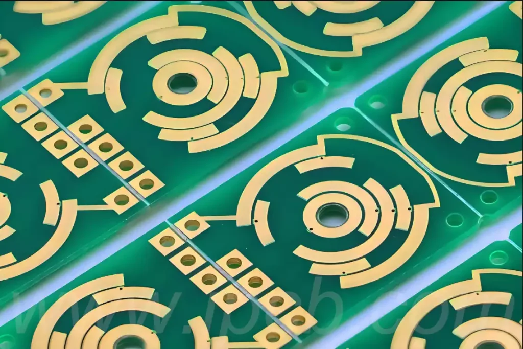
The difference between graphic transfer and graphic plating:
- Different purposes: the purpose of the transfer of graphics is to transfer the circuit pattern to the pcb board,while the purpose of the graphic plating is to increase the thickness of the copper layer of the conductive region.
- Technical means: graphic transfer mainly uses photolithography, while the graphic plating uses electrochemical methods.
- Material use: graphic transfer using photoresist, while graphic plating using copper ions in the plating solution.
- Production results: after the completion of the graphic transfer, the outline of the circuit pattern has been formed, but the conductive properties have not yet been enhanced; graphic plating is completed, the thickness and performance of the conductive path has been significantly improved.
- Production sequence: graphic transfer is a step before the graphic plating, without graphic transfer, graphic plating can not be carried out.
Double sided pcb board graphic transfer and graphic plating technology together constitute the core of the double sided PCB manufacturing, the former to ensure that the pattern is accurately reproduced,the latter to enhance the conductive properties, the two complement each other to promote the continuous progress of pcb board manufacturing technology.
