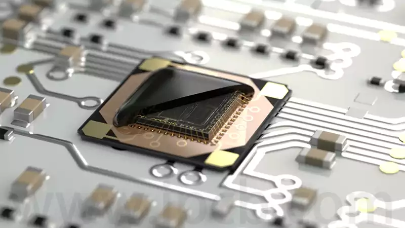
PCB encapsulation materials consist of substrates, interconnections, frames, interlayer media, and sealing materials. Among these, PCB encapsulation substrate materials serve as electronic components, primarily providing mechanical support, hermetic protection, and facilitating heat dissipation for electronic components and their interconnections.
Substrate: High-density multilayer encapsulation substrates primarily serve as an electrical transition between semiconductor chips and conventional PCBs (printed circuit boards), while also providing protection, support, and heat dissipation for the chips. Primary materials include ceramics, epoxy glass, diamond, metals, and metal-based composite materials.
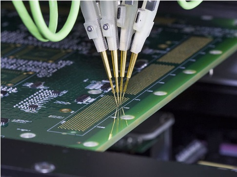
Interconnections: Conductor interconnections are formed through a metallisation process. Substrate metallisation is performed to mount the chip on the substrate and connect it to other components.
Interlayer Dielectrics: Dielectric materials play a crucial role in electronic packaging, including circuit protection, insulation, and prevention of signal distortion.
Sealing materials: Sealing materials for electronic devices and integrated circuits are primarily ceramic and plastic. The earliest materials used for packaging were ceramic and metal. As the circuit density and functionality of electronic products have gradually increased, the requirements for packaging technology have also become more stringent, leading to a shift from metal/ceramic packaging to plastic packaging. Currently, epoxy resin-based sealing materials account for approximately 90% of the market share in circuit substrate density materials.
PCB encapsulation materials should meet the following performance requirements:
High thermal conductivity to ensure electronic components are not damaged by heat
A thermal expansion coefficient matching that of the chip to prevent chip failure due to thermal stress
Excellent high-frequency characteristics to meet high-speed transmission requirements
Common PCB encapsulation materials include plastic, metal, and ceramic, with the specific choice depending on the characteristics of the circuit board and the application scenario.
Plastic packaging materials
Plastic packaging materials are widely used in electronic circuit board packaging, with primary advantages including low cost, ease of processing, lightweight, and good thermal insulation. There are numerous types, with the most common being:
Epoxy resin: Epoxy resin is renowned for its excellent mechanical strength and adhesion, making it widely used. It offers high moisture resistance and chemical resistance, with a dielectric strength typically around 15–25 kV/mm. However, they may be rigid and may crack under extreme thermal cycling.
Silicone gel: Silicone gel is flexible and well-suited for applications requiring thermal expansion or vibration damping. It performs well over a wide temperature range (typically -60°C to 200°C) and provides excellent moisture protection.
Polyimide (PI): High-temperature resistant and radiation-resistant, suitable for encapsulation materials used in high-temperature environments.
Plastic systems: Such as polystyrene (PS), polycarbonate (PC), epoxy resin (EP), etc., these materials have good mechanical properties and weather resistance, and are generally used for producing housings or frames.
Engineering plastics: such as polyamide (PA), polypropylene (PP), nylon (NY), etc. These materials have good heat resistance, toughness, and corrosion resistance, and are widely used in harsh application environments.
Metal Enclosure Materials
Metal enclosure materials are widely used in special applications due to their excellent thermal conductivity, resistance to electromagnetic interference (EMI), high-temperature resistance, high strength, and corrosion resistance.
Steel Enclosures: Typically used in the manufacture of high-quality servers, switches, and other high-performance equipment.
Aluminium Enclosures: These have excellent heat dissipation properties and are suitable for packaging low-power devices.
Magnesium Alloy Enclosures: These have low density, high strength, and good mechanical properties, making them suitable for packaging lightweight products such as tablets.
Ceramic Packaging Materials
Ceramic packaging materials have excellent high-temperature resistance and mechanical strength, making them widely used in electronic devices that operate at high temperatures or frequencies.
Al₂O₃ ceramic substrates
Alumina ceramics are the most mature ceramic substrate materials currently in use. Their advantages include low cost, good thermal shock resistance, and excellent electrical insulation properties, with mature fabrication and processing technologies. As a result, they are widely used in the electronics industry, accounting for 90% of all ceramic substrates, and have become an indispensable material in the electronics industry.
AlN ceramic substrates
AlN ceramic substrates are a new type of substrate material with excellent electrical and thermal properties. Compared to alumina, they have a higher thermal conductivity (generally more than five times that of alumina ceramics), making them suitable for high-power, high-lead count, and large-size chips. Additionally, AlN is a hard material that can operate under harsh environmental conditions, enabling the production of very thin substrates to meet the requirements of various packaging substrates. However, its drawbacks include complex preparation processes and high costs, which limit its large-scale production and application.
BeO ceramic substrates
The most notable feature of beryllium oxide ceramic substrates is their extremely high thermal conductivity, which is comparable to that of metallic materials. Among currently available ceramic materials, BeO has the highest thermal conductivity at room temperature and also serves as an excellent insulating material. BeO has a low dielectric constant, low dielectric loss, and strong adaptability to packaging processes. The biggest drawback of BeO is its high toxicity, which requires special protective measures during preparation and higher processing temperatures, resulting in high costs and significant environmental pollution, thereby limiting its production and widespread application.
BN Ceramic Substrates
Boron nitride (BN) is commonly used in radar windows, high-power transistor sockets, housings, heat sinks, and microwave output windows due to its high thermal conductivity, which remains nearly constant across temperature ranges, low dielectric constant, and excellent insulating properties. However, cubic boron nitride is expensive and unsuitable for producing high-thermal-conductivity ceramics typically used in applications; and its thermal expansion coefficient is incompatible with silicon, further limiting its application.
Why is PCB encapsulation or potting necessary?
Electronic devices are often exposed to conditions that can reduce their performance or cause complete failure. From industrial machinery operating in humid environments to automotive systems facing extreme temperatures, unprotected PCBs are vulnerable to attack. Here are some key reasons why encapsulation or potting is essential:
Moisture and water resistance: Moisture spray or humidity can cause PCB short circuits or corrosion. Encapsulation forms a waterproof seal, preventing water ingress and ensuring electronic devices remain functional even in humid conditions.
Resistance to environmental hazards: Dust, dirt, and corrosive chemicals are common environmental hazards that can damage exposed components. A protective layer keeps these elements at bay, extending the device’s lifespan.
Impact and vibration resistance: In applications such as aerospace or automotive systems, PCBs are subjected to continuous vibration or sudden impacts. Encapsulation absorbs mechanical stress, reducing the risk of loose connections or component fractures.
Thermal management: Some encapsulation compounds aid in heat dissipation, protecting components from overheating. For example, certain epoxy resins have a thermal conductivity range of 0.2 to 1.5 W/m·K, helping to transfer heat away from critical areas.
Preventing electrical issues: PCB encapsulation materials with high dielectric strength (epoxy resins typically exceed 20 kV/mm) prevent arcing or corona discharge in high-voltage applications, ensuring safety and reliability.
By addressing these challenges, PCB encapsulation ensures that electronic devices can operate reliably in harsh environments, from underwater sensors to outdoor communication equipment.