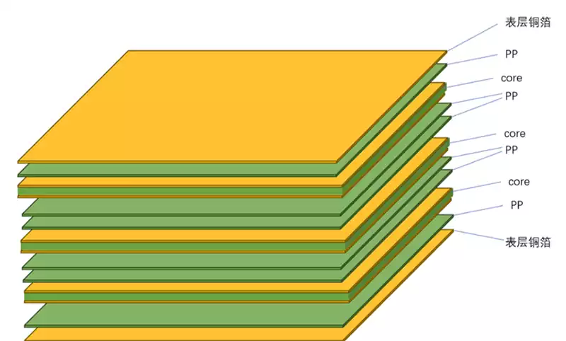
The PCB laminate structure primarily comprises three key base materials: copper foil, prepreg (semi-cured sheet), and core board (also known as substrate). Taking a common 8-layer PCB laminate structure as an example, the uppermost layer is the surface copper foil, followed sequentially by prepreg, core, with prepreg and core alternately stacked, and the bottom layer being copper foil. It is noteworthy that PCB layer counts are invariably even; odd-numbered layers do not exist.
- Copper Foil
Copper foil serves as the critical material for conductor traces on the TOP (top layer) and BOTTOM (bottom layer) of multilayer boards. Common thickness specifications for surface copper foil include three types: 12μm (1/3oz), 18μm (1/2oz), and 35μm (1oz). Following processing, the final thickness typically measures approximately 44μm, 50μm, and 67μm, roughly corresponding to copper thicknesses of 1oz, 1.5oz, and 2oz (1oz equates to approximately 35μm). - Prepreg
PP board, fully termed Prepreg, essentially constitutes a semi-solid ‘intermediate bonding layer’. Accurately speaking, it is not a “board” but rather a ‘bonding filler material’. It comprises components such as fibreglass cloth and resin (e.g., epoxy resin). Within PCB boards, PP boards are sandwiched between the core board and copper foil, or positioned between two core boards, serving as a dielectric layer providing insulation. - Core
The core, commonly termed ‘Core’, is fundamentally a solid ‘foundational sheet material’. It is produced by impregnating fibreglass cloth or other reinforcing materials with resin, then laminating copper foil to one or both sides before hot pressing into a solid sheet material. Among these, FR4 (“FR” denotes ‘Flame Retardant’; ‘4’ denotes the industry classification code) is a specific grade of substrate (Core) and currently the most widely used substrate type in PCB board applications.
The key distinction between Core and PP lies in their physical form: Core exists as solid sheets (requiring cutting into individual pieces for use) with copper foil laminated on both sides; PP, conversely, is supplied as flexible rolls without copper foil, serving solely for bonding and filling purposes.
FR-4
FR4 (‘FR’ denotes ‘Flame Retardant’; “4” is the industry classification code) is a commonly used material for pcb boards. It is typically composed of a ‘Tera-Function Epoxy’ matrix, reinforced with fillers and composite glass fibre cloth. The dielectric constant of FR4 laminates ranges between 4.2 and 4.7, with variations depending on the specific prepreg type. Furthermore, the dielectric constant decreases with increasing frequency. Consequently, during layout design, impedance is typically controlled empirically. Following Gerber file generation, the PCB manufacturer will perform minor adjustments to the stack-up line widths and spacings.
Another crucial characteristic of FR4 is its glass transition temperature (Tg). This denotes the temperature at which the material transitions from a relatively rigid or ‘glass’ state to a deformable or softened state. This parameter directly determines the PCB’s temperature resistance and dimensional stability—a higher Tg value indicates superior temperature tolerance, making it particularly suitable for lead-free soldering processes.
Tg Classification (Conventional Standards)
Standard Tg Material: Tg > 130°C (Representative Model: Shengyi S1141);
Medium Tg Material: Tg > 150°C (Representative Model: Shengyi S1141 150);
High Tg Material: Tg > 170°C (Representative Model: Lianmao IT180A).
Differences Between Multilayer and Single-Layer PCB Boards
During the manufacturing process of multilayer PCB boards, the method of circuit formation differs little from that of single-layer or double-layer circuit boards. However, the via fabrication process is markedly distinct. Circuits are formed through etching, whereas vias are created by drilling followed by copper plating.
Multilayer circuit boards are typically categorised into through-hole boards, first-order boards, second-order boards, and second-order stacked-via boards. Although higher-order products like third-order boards and arbitrary-layer interconnect boards are relatively uncommon in the market and command premium prices, understanding their fundamental characteristics is crucial for comprehending multilayer PCBs.
In practical applications, 8-bit microcontroller products typically employ 2-layer through-hole boards; whereas 32-bit microcontrollers and higher-end smart hardware opt for 4- to 6-layer through-hole boards. For Linux and Android system-level smart hardware, 6-layer through-hole to 8-layer HDI boards prove more suitable; compact products like smartphones predominantly utilise 8-layer first-order to 10-layer second-order pcb boards.
Through-Hole Boards vs. HDI Boards
Through-holes represent the most prevalent type of via configuration. In this structural form, the via penetrates the entire stack-up from the first layer to the last, with the aperture fully penetrated regardless of whether it connects external or internal traces. Boards featuring this via structure are termed through-hole boards, distinguished by their exceptional connectivity and electrical continuity.
There is no direct correlation between the number of layers in a PCB board and its classification as a through-hole board. For instance, the commonly used two-layer PCB boards in everyday applications are typically through-hole boards. Conversely, pcb boards for switches or those employed in military applications often feature 20 layers or more, yet may still utilise through-hole design methodologies.
In the PCB manufacturing process, through-holes are created by drilling holes through the board using a drill bit. Copper is then plated inside these holes to form conductive pathways. It is worth noting that common inner diameter specifications for through-holes include 0.2mm, 0.25mm, and 0.3mm. However, vias with a 0.2mm ID are generally more expensive. This is primarily because using finer drill bits increases the risk of bit breakage and results in slower drilling speeds, consequently extending manufacturing time and costs.
Additionally, high-density interconnect (HDI) boards employ laser drilling technology to create holes. This method enables more precise control over hole positioning and dimensions. In HDI boards, the inner layers employ mechanical drilling, following a design principle similar to that of a four-layer through-hole board: mechanical drilling is completed internally, with two additional layers overlaid externally. It is important to note that laser drilling can only penetrate glass fibre laminates and cannot penetrate the copper metal. Therefore, laser drilling on the outer surface of the circuit board does not interfere with other internal circuits. Following laser drilling, a copper plating process is applied to form the laser vias.
Second-level HDI boards employ dual-layer laser drilling to create apertures, each with a diameter of 0.1mm. This design yields finer holes, significantly enhancing the board’s precision and performance. Concurrently, laser drilling ensures precise hole positioning and consistency between holes, providing a robust foundation for subsequent circuit connections.
The PCB laminate is built upon a stable foundation of three primary substrates: copper foil, polypropylene (PP), and the substrate material. While manufacturing processes share commonalities across different PCB layer counts, through-hole boards and HDI boards exhibit distinct performance characteristics due to their unique via formation methods.