What is pcb panelization?PCB panelization refers to the process of integrating several small PCB boards into one large board by the manufacturer. From the initial stage of PCB design until the final production link, the board assembly operation always plays a pivotal role. It is not only about the quality of the PCB board to meet the standards, but also profoundly affects the cost-effectiveness of PCB production.
PCB panel size requirements:
① For small single board, when its size is less than 100mm × 70mm, the need for board processing. The dimensions of the board should meet the following conditions: the length L should be in the range of 100mm to 400mm, the width W should be between 70mm to 400mm.
② The design of the direction of the board should be consistent with the direction of the transfer edge as much as possible, unless it is impossible to meet the above requirements due to size constraints.
③ For irregularly shaped PCBs, process edges should be added. When processing, make sure that the connection between the process edge and the PCB is not arranged with any devices and lines to ensure the smooth operation of soldering and cutting.
④ Inside the patchwork board, the number of connection points (e.g. V-CUT or stamp holes) between small boards should be controlled within a reasonable range (no more than 3) to ensure the smoothness of the cutting and separation process.
pcb panelization rules:
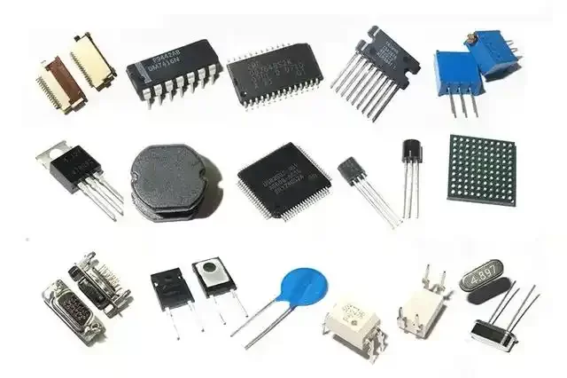
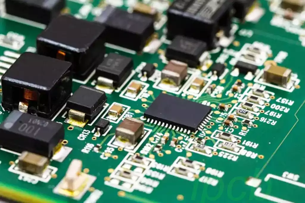
In order to reduce the board gap, components with the same size and package should be prioritized and combined together.
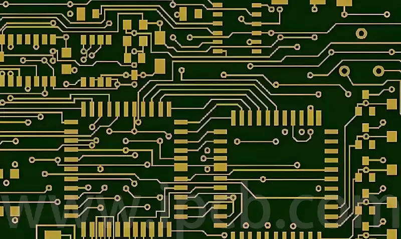
Sufficient spacing between components should be maintained to facilitate subsequent assembly, maintenance and to ensure electrical isolation.
When panelization the board, it is necessary to strictly refer to the design drawings of the devices to ensure that the electrical connections are accurate, especially the power and ground connections, to prevent short circuits and other failures.
To reduce electromagnetic interference between components and edges, the distance from components to metal edges should be minimized.
To reduce interference, components should be avoided to cross each other arranged.
PCB panelization skills:
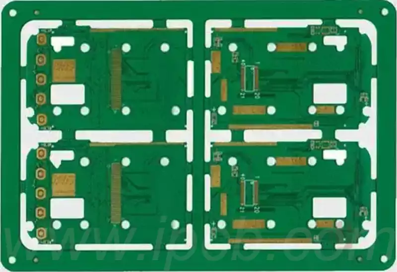
The peripheral edges (i.e., the clamping area) of the PCB panelization need to be designed as a closed-loop structure to ensure that the panelization board maintains its shape stability when it is fixed in the fixture. The width of the board should not exceed 260mm (for SIEMENS production line) or 300mm (for FUJI production line). If automatic dispensing is required, the product of width and length of the board should be no more than 125mm×180mm. the shape of the board should be as close to square as possible, and it is recommended to use 2×2, 3×3 and other specifications of the board, but it is necessary to avoid the yin and yang design of the board. The center distance between small boards is recommended to be controlled between 75mm and 145mm.
When setting the reference positioning point, a non-resistance welding area 1.5mm larger than the positioning point should be retained around it. Large or protruding components should be avoided around the connection points between the outer frame of the board and the internal small boards, as well as between the small boards, while the distance between the components and the edge of the PCB board should be greater than 0.5mm to ensure the smooth operation of the cutting tool.
Four positioning holes should be opened at the corners of the outer frame of the board, the aperture should be 4mm ± 0.01mm, the strength of the holes need to be moderate, in order to prevent breakage in the process of up and down the board. Positioning hole diameter and positional accuracy should be high, the hole wall should remain smooth without burrs. Each small board within the patchwork should have at least three positioning holes, the aperture should be between 3mm to 6mm, and the edge of the positioning holes within 1mm shall not be wired or patch.
For the PCB board positioning and fine pitch device positioning reference symbols,in principle,the pitch is less than 0.65mm QFP should be set in its diagonal position positioning reference symbols.The positioning reference symbols used for PCB sub-boards should be used in pairs and arranged at the diagonal of the positioning elements.
The PCB panelization technology combines strict rules and practical skills, which are crucial to ensure the quality of the board, optimize production costs and enhance the efficiency of subsequent assembly. Mastering these rules and techniques will effectively enhance the design and production level of PCB panelization.