PCB pins are the metal parts of printed circuit boards used to connect electronic components. They are usually small metal columns or pads extending vertically from the surface of the PCB board, through welding, plugging and other ways and components of the pins or pin holes are closely linked to realize the transmission of circuit signals and the distribution of electrical energy. Although the pin is small, but as the human body in the nerve endings, transfer control instructions and energy flow, is the basis for the realization of the function of electronic equipment.
Types of electronic device pins include inline pins, SMD pins, modular pins and other types.
Inline pins
Inline pins are the most common type of pins, which are usually presented in the form of directly inserted into the circuit board, and some inline pins need to be connected to the circuit board through the socket, which is usually used for chip-level components. The shape of the straight pin is usually about 0.5 mm in diameter inwardly curved “U” shaped design, this pin connection is stable, the contact area is large, in the industrial production line is easy to install, easy to detect.
SMD pins
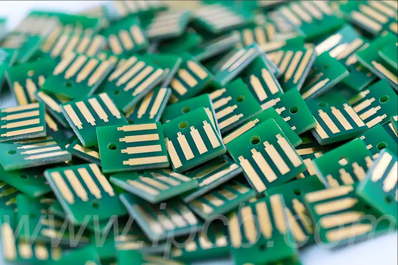
SMD pins are one of the most common types of pins in modern electronic devices. It is usually used on smt surface mount circuit boards, so it is also called smt pin. SMD pins are rectangular in shape and may be presented in different sizes and arrangements. Depending on the application, there may be 1,2,4,6,8,10 and 20 pins, etc. The different sizes of SMD pins have different names, and there are different types of SMD pins, such as SOP, QFN, LCC, and DIP, etc. The smaller sizes of SMD pins make the whole circuit design more compact and lightweight. The smaller size of SMD pins can make the whole circuit design more compact and lighter.
Modular pins
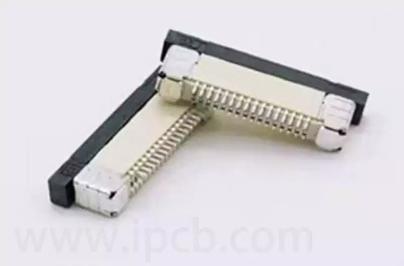
As electronic devices become more and more common, more and more complex modular circuit designs emerge. In order to more easily connect the different modules of the circuit, modular pins began to be widely used. The modular pin form factor is usually an inline or stick-on pin, but uses standard interfaces and electrical characteristics for easy connection and replacement. Common modular pin standard USB, RJ-45, PCI, PCMCIA and so on.
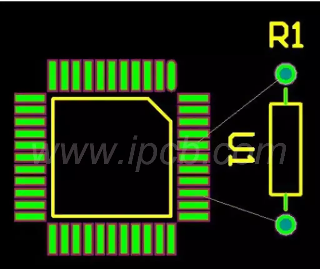
The clearance between the test point and the pin through-hole is an important parameter in PCB design.
The minimum pitch D is 125 mil: this is the minimum acceptable clearance between the test point and the pin via. This gap is to ensure that there is enough space between the test points and the pin vias so that they do not come into contact with each other or short-circuit.
The gap between the test point and the pin through-hole is to ensure that the test point can connect properly to the pin through-hole and provide a stable and reliable connection. Larger gaps provide better safety and reduce the risk of potential failures.
However, it is important to note that larger gaps may take up more space and may impose certain constraints on the layout and size of the PCB board. Therefore, design requirements and constraints need to be taken into consideration when determining the clearance between test points and pin through holes.
It is recommended to work with the manufacturer and design team during the PCB design process to determine the appropriate clearance between test points and pin through holes and to ensure that design and manufacturing requirements are met. This ensures a reliable connection between the test points and the pin-through holes, as well as proper performance and reliability of the board.
How to set up pins for a PCB schematic
- Mark the pins: Give each pin a unique identifier.
- Arrange pins: Arrange the pins in a logical order according to the function and layout of the pcb components.
- Assign Pin Types: Determine the type of pin based on the function of the component. Ensuring that the pin types are correctly assigned helps to connect the circuit correctly.
- Add labels and comments: Add labels and pcb comments to explain the purpose of the pins and how they are connected, if needed.
- Connect pins: Connect pcb board pins together to form a circuit by using symbols and wires.
- Refer to specifications: If you are designing a circuit board schematic for a specific project or industry standard, make sure you follow the appropriate specifications and requirements.
Things to consider when selecting pcb board pins
- Type
Obviously, you need to determine the type of PCB pins that are appropriate for your design. If you are looking for terminal pins for board-to-board connections, rows of pins are the right choice. Row pins are usually through-hole mounted, but there are also surface mounted versions that are ideal for automated assembly.
In recent years, solderless technology has provided more options for printed circuit board pins. Press-fit pins are ideal for eliminating solder. They are designed to fit into padded PCB holes and provide secure mechanical and electrical continuity. Single row row pins are used for board-to-board and wire-to-board.
- Pitch
Some printed circuit board pins are available in a variety of pitch sizes. For example, double rows of pins are typically available in 2.54mm, 2mm and 1.27mm. In addition to the pitch size, individual pin dimensions and current ratings vary. - Material
The material used for plated pins may result in different costs and conductivity. Gold-plated pins are usually more expensive than tin-plated pins, but have higher conductivity.
The importance of pcb pins, as the precision building blocks of the electronic world, cannot be overstated. As technology continues to advance, pin design and application will continue to innovate for the high performance and reliability of electronic products.