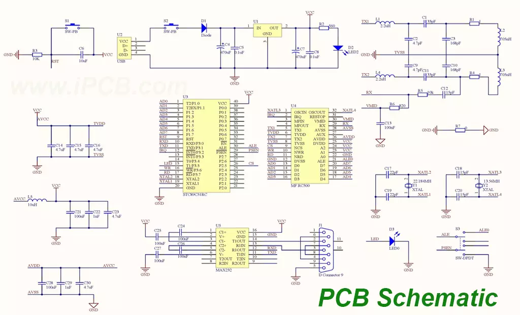
PCB schematic, as a drawing that describes how the various components of a circuit board are connected, is a fundamental tool for electronic engineers to design and analyze circuits. Also known as a circuit schematic or circuit diagram, it is a drawing that uses graphic symbols to represent the connection relationships of a circuit. Through the schematic diagram, engineers can clearly understand the connection relationship and working principle of each component in the circuit, to analyze and optimize the performance of the circuit. Circuit diagrams are an important part of electronic design automation (EDA) and are important for PCB layout, wiring, and electronic product development.
PCB Schematic Drawing software
There are many excellent circuit schematic drawing software on the market, such as Altium Designer, Eagle, Multisim, and so on. This software is powerful, easy to learn, and easy to use, to meet the needs of engineers at different levels.
Altium Designer is a professional printed circuit board design software with the following advantages:
Rich component library: Altium Designer provides a large number of standard component libraries, easy for users to find and call a variety of component symbols.
Powerful circuit simulation: the software has a variety of built-in simulation tools to help engineers in the schematic design stage of the circuit simulation and verification.
Automatic wiring function: Altium Designer has an automatic wiring function, that can greatly improve the efficiency and accuracy of circuit board wiring.
Visualization tools: the software provides a wealth of visualization tools to facilitate engineers to observe and analyze the circuit.
Multi-platform compatibility: Altium Designer supports a variety of operating system platforms, which is convenient for users to use on different operating systems.
PCB Schematic Drawing Method
Create a new project: Open Altium Designer software, create a new project, name the project, and choose a storage location.
Add component libraries: In the project browser, right click the “Libraries” folder, and select “Add Library” to add the required component libraries. Depending on your needs, you can choose from the libraries that come with the software or import them from third-party libraries.
Placement of components: In the schematic editing interface, drag and drop components from the component library to place them on the drawing. According to the needs of circuit design, select the appropriate component symbols and place them in the appropriate locations.
Connect Components: Use the line tool to connect components to indicate the electrical relationship between them. According to the requirements of the circuit design, rationally plan the direction and layout of the connecting lines.
Add notes and text: When necessary, add notes and text to the schematic to explain what the components do and how they are connected. This helps to improve the readability and understanding of the schematic.
Save and Export: After completing the schematic, save the project and export it to a commonly used format such as PDF or image. This allows you to share the schematic with others or use it for printed circuit board fabrication.
how to convert PCB schematic to pcb layout in Kicad
The process of converting a printed circuit board schematic diagram to a PCB layout in KiCAD can be broken down into the following steps:
Open the KiCAD software and load the schematic file.
Check the components and connections in the schematic to ensure that there are no errors or omissions in the schematic.
Determine the PCB dimensions and layout requirements, such as layers, component packages, wiring rules, etc.
Load the PCB frame file and define the boundaries and dimensions of the wiring boards.
Import the components and connections from the schematic into the PCB layout. This can be done by using KiCAD’s import function or by manually copying and pasting components and connections.
Adjust the position and orientation of the components and add the necessary PCB component packages according to the PCB layout requirements.
According to the wiring rules, use KiCAD’s wiring tools to perform wiring and establish the connection relationship between components.
Perform DRC verification on the PCB to check if the board complies with the design rules. If there is any problem, you need to adjust and modify the PCB.
Export the PCB file to DXF, PDF, SVG, etc. for further processing or printing in other software.
The use of circuit schematics mainly includes the following aspects:
Circuit analysis and design: circuit schematic is the basis for circuit analysis and PCB design. Through the schematic diagram, engineers can clearly understand the connection relationship and working principle of each component in the circuit, to conduct circuit performance analysis and optimization. In this process, the schematic diagram can provide intuitive and accurate information to facilitate engineers to better understand the working principle of the circuit and the design intent.
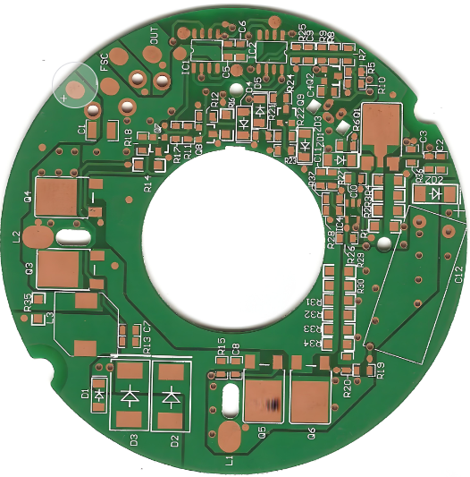
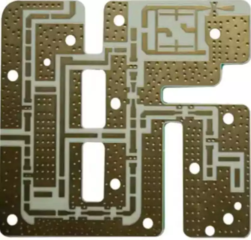
Production of circuit boards: it is the basis for the production of printed circuit boards. According to the schematic diagram, you can determine the location and connection of each component in the circuit, to carry out the layout and wiring of the circuit board. In the production process, the schematic diagram can provide guidance and reference for the production of circuit boards to ensure that the performance and reliability of the circuit board meet the design requirements.
Development and debugging of electronic products: it is an important tool for the development and debugging of electronic products. Through the schematic diagram, it is easy to simulate and verify the circuit to check the correctness and reliability of the circuit. At the same time, in the process of product development and debugging, the schematic diagram can provide engineers with intuitive and accurate information to facilitate engineers to better understand the performance and characteristics of the product.
Technical support and maintenance: In the production and maintenance of electronic products, PCB schematic diagrams can be used as an important basis for technical support and maintenance. If the product malfunctions or problems, engineers can quickly locate the problem through the PCB schematic diagram, determine the solution, and repair and improve. In this process, the PCB schematic can provide accurate and reliable information to improve the efficiency and accuracy of technical support and maintenance.