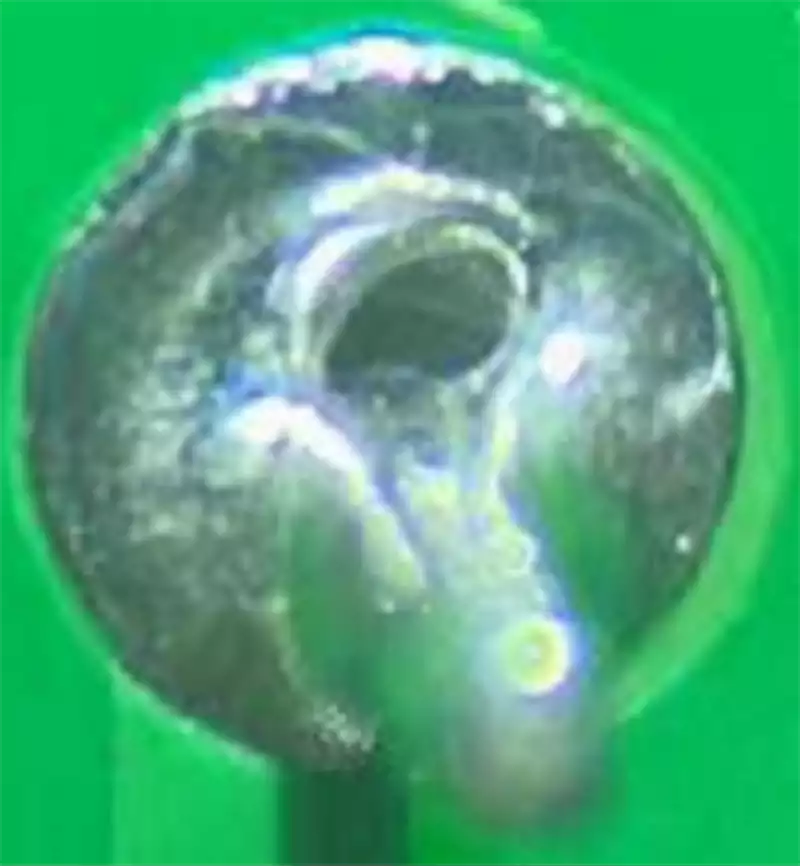
Solder blow hole refers to the plug-in over the wave soldering, the hole in the gas due to high temperature and out of the solder, so that the hollow formed in the solder. Due to high temperature and high humidity, plating quality, organic pollutants and other reasons caused by plug-in solder joints blow holes, often leading to poor PCBA welding, affecting product reliability.
In the wave soldering production process, solder blow holes is a relatively common defective phenomenon, that is, from the surface of the solder joints visible to the naked eye a larger cavity, in IPC-A-610 is defined as the need to improve the item.
The core root cause of the solder blow hole defects on PCBs lies in the quality of the PTH (Plated Through Hole) plated holes, which mainly involves drilling and copper plating. Problems in the drilling process can cause the hole wall to become rough and uneven; while poor copper plating is mainly reflected in the copper layer thickness fails to meet the standard value and uneven distribution of copper layer thickness. In addition, if the cleaning step after drilling is not carried out thoroughly, plate powder or other impurities will be left in the holes, and these residues will further affect the quality of copper plating, and ultimately form cavities in the hole wall. In order to accurately identify these problems, slicing of defective solder joints is considered to be the most effective means.
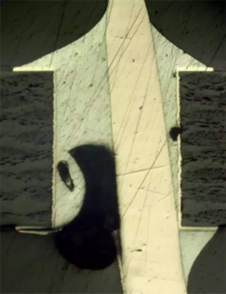
From the sliced image, it can be clearly observed that the thickness of the copper layer inside the hole wall is thin and accompanied by the presence of significant voids, which are already observed in the cooling state. In the wave soldering process, when the board is heated, the copper layer undergoes longitudinal tensile deformation due to the coefficient of thermal expansion (CTE) in the Z-direction. Thin copper layers are prone to fracture, and the condition of already existing voids is worsened. At the same time, the moisture inside the sheet is converted to vapour at high temperatures, and this vapour force ‘squeezes’ the solder outwards, leading to the formation of blowholes.
Solution:
1.Strengthen the inspection of the drill, once found that the drill dull should be replaced immediately to avoid drilling surface roughness, thereby improving the overall quality of drilling.
2.Strengthen the cleaning of each process, especially to ensure that the powder and foreign matter generated after drilling are thoroughly removed, to avoid them remaining in the hole, which will have a negative impact on the quality of the subsequent plated holes.
3.Improve the quality of copper plating of PTH plated holes to ensure that the minimum and average thickness of the copper layer meets the requirements of the relevant IPC standards. For example, for level 2 products, the minimum thickness of the copper layer should be no less than 18µm and the average thickness should be no less than 20µm.
4.Strengthen the baking link during PCB processing, and strictly control the moisture content of the board to reduce the impact of moisture on the soldering quality.
5.Pay attention to the printing accuracy of solder resist ink to avoid printing offset resulting in contamination of the plated holes, which in turn affects the quality of wave soldering solder joints. In extreme cases, the printing offset may even completely destroy the functionality of the plated holes.
PCB solder blow hole defects, as a common problem in wave soldering production, not only affect the appearance of the quality of the solder joints, but also pose a potential threat to the reliability and long-term stability of the product. In the future, with the continuous progress of electronic manufacturing technology and consumers’ increasing demand for product quality, the prevention and control of PCB blow-hole defects will be even more stringent. Therefore, the continuous exploration and optimisation of solutions will be the eternal theme of the electronics industry.