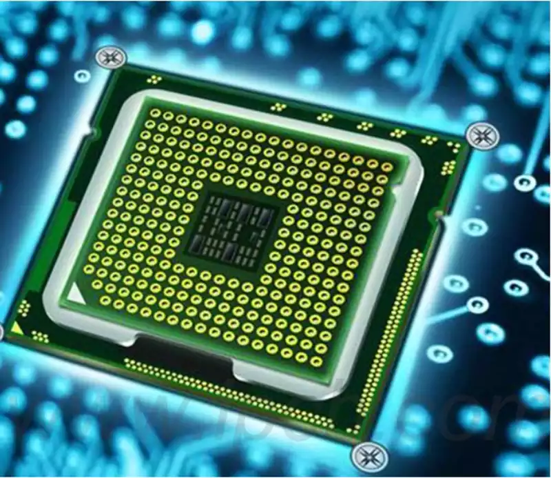
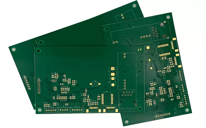
PCB substrate key components in the electronics field that utilize chemical etching technology to connect electronic components (e.g., wires, resistors, capacitors, etc.) to copper foil to form a complete circuit system. This technology allows for the smooth transmission of signals and currents between electronic components, thus ensuring the proper functioning of electronic devices.
Packaged substrates focus on encapsulating electronic components (e.g., wafers, resistors, capacitors, etc.) on a homogeneous substrate and securing the components through soldering and other processes. Its design and manufacturing process needs to fully consider the layout of the components, connecting lines and heat dissipation and other factors, designed to provide physical protection for electronic components, and to ensure the stability of the circuit electrical connection.
PCB substrate in electronic equipment plays multiple roles, it not only realizes the electrical connection between electronic components, but also provides mechanical support and thermal management functions. Through the carefully designed conductive track, it can realize a variety of complex circuit connections, to ensure that the signal and current transmission between the electronic components is accurate. At the same time, the material and structural design of the PCB plate ensures sufficient mechanical strength and stability to effectively support and protect the electronic components. In addition, it effectively disperses and conducts the heat generated to maintain the normal operating temperature of the electronic equipment.
Differences between substrate and PCB
From the point of view of the application environment and function, the substrate is mainly used as the support of electronic components, its structure and manufacturing technology is relatively simple, can be made into different shapes and sizes. PCB, on the other hand, is mainly used to realize the conductivity and isolation of the circuit, and its structure and manufacturing process is relatively complex, requiring higher precision and quality control.
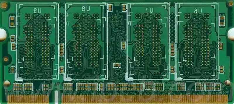
The uses of both are also different. Substrate is mainly used to support electronic components, while the circuit board is coated with conductive substances on the surface to achieve a variety of components of the circuit connection and signal transmission, can be generated at different levels and complexity of the circuit, is widely used in various types of electronic equipment, computer accessories and communications equipment manufacturing.
There are also differences in production processes. Substrate manufacturing typically involves processes such as molding, stamping, drilling, copper plating, polishing and slotting, while PCBs require more elaborate manufacturing techniques such as etching and chemical copper plating, as well as wiring, soldering and other processes. These differences in manufacturing technologies lead to differences in manufacturing costs and scope of use.
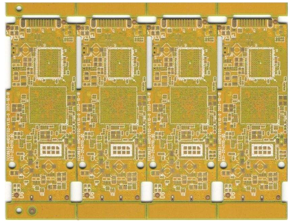
In terms of application scenarios, PCBs are mainly used as connectors for electronic devices to connect various electronic components such as wafers, resistors and capacitors. Substrates, on the other hand, are more often used on integrated circuit (IC) wafers as a support and connection carrier for the wafers.
Although both package substrates and PCB substrate plays an important role in the construction of electronic devices, they differ significantly in terms of function, purpose, production process and application scenarios. An in-depth understanding of these differences helps us to more accurately select and use these critical components to optimize the performance and reliability of electronic devices.