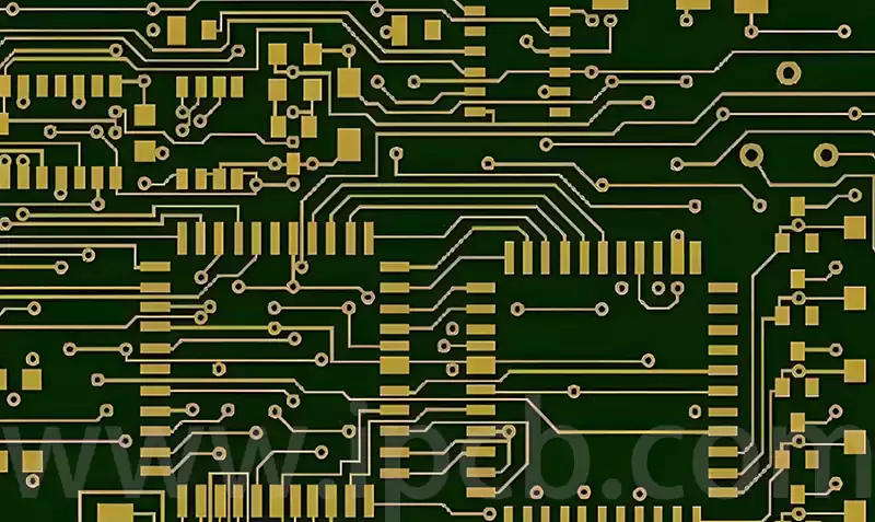
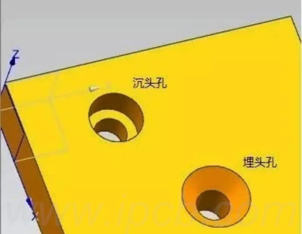
PCB via filling technology mainly refers to the use of specific filler materials to fill through holes (such as through holes, mounting holes, etc.) in the PCB manufacturing process, in order to realize the electrical connection between the layers of the circuit board or structural fixation. The selection of filler materials and the control of the filling process is critical to ensure the quality and performance of the PCB.
Through-hole filling technology is a complex process, mainly including the following steps:
- Drilling: According to the design requirements and standards, drill holes on the PCB board to form the required through-holes.
- Chemical cleaning: use appropriate solvents to clean off the oil and impurities on the through-hole board, and then use acidic or alkaline solutions for corrosion treatment to remove the oxide layer on the surface of the through-hole board to improve the adhesion of plating.
- Pre-plating treatment: activate the through-hole plate to make its surface with good conductivity, and then degreasing treatment to remove residual oil and impurities, to ensure that the through-hole plate surface is clean and smooth.
- Plating hole filling: Fill the through holes with conductive materials, such as copper, to form a continuous conductive path. The filling material can be liquid or solid, and the filling method can be chemical deposition, electroplating or hot pressing.
- Surface treatment: the filled through-hole surface treatment, such as grinding, polishing, etc., so that its surface is smooth and flat to meet the subsequent process requirements.
Some common methods of filling through-holes include:
- Through tenting
Through-hole tenting creates a soldermask layer over the PCB board through-hole instead of filling the hole with material. This can be a quick, easy and cost-effective alternative to covering the via hole, but tented vias may re-open over time. - Through Plugging
The through-hole plugging process fills the hole with a non-conductive material and seals it with a mask. Through-hole plugging also covers the ring and does not produce a smooth, glossy surface. - Through-Fill
Through-hole filling uses resin to create a permanently filled hole. Through-hole filling is a common type of through-hole filling in which the manufacturer fills the through-hole with a conductive material, plates the surface with copper, and then trims the surface. This process allows signals to be routed to other areas of the PCB.
Applications of pcb via filling
Saving space
Protects solder floating to the electronic component side
Facilitates stacking and interleaving of microvias for sequential build-up of multilayers (SBU)
Facilitates in-pad through-hole technology, e.g. BGAs
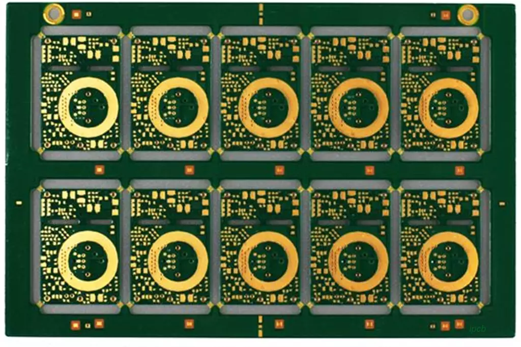
Role of pcb through holes
- Simplify circuitry: Through-holes allow current to flow through without the need for additional conductors or contacts, thus reducing circuit complexity and effort.
- Improve signal transmission: Through the vias, signals can be transmitted from one place to another, reducing signal interference and distortion.
- Improve package density: Through-hole can reduce the number of components on the PCB, thereby increasing the density of the new circuit and reducing the size of the PCB.
- Reduce manufacturing costs: Vias do not require additional manufacturing costs because they are a natural part of the PCB design.
- Increase flexibility: Vias can be used to connect different component types and locations, providing more design flexibility.
- Improve reliability: Vias can prevent short circuits and open circuits between components, thus improving circuit reliability.
PCB via filling technology is a key technology indispensable to the electronics manufacturing industry. With the continuous development of electronic products and changes in market demand, it will also continue to develop and innovate, injecting new momentum into the future development of the electronics manufacturing industry.
