In the field of electronics manufacturing, PCBA chip processing constitutes a core link in the product manufacturing process, and plays a decisive role in the performance, stability and durability of electronic products. Stability and durability play a decisive role in the performance of electronic products, stability and durability.PCBA chip processing of pcb boards set a very high standard, these standards have a direct impact on the subsequent assembly quality and product performance. In order to ensure the smooth processing of the chip, PCB must meet a series of critical requirements.
PCBA chip processing PCB boards need to meet several core welding standards
Welding quality requirements
Soldering as the core link in PCBA chip processing, its reliability is deeply affected by the quality of the PCB board. For welding quality, PCB boards need to meet the following key standards:
- Accuracy of pad design
PCB pad design should be strictly based on the size of the component and its package type for accurate planning. Too large or too small a pad size may cause instability of the soldering point, resulting in false soldering or cold soldering phenomenon, which in turn adversely affects the electrical performance of the product. Following the IPC-2221 standard,the pad size should match the component pin size to ensure that the soldering area can be fully contacted. - Appropriateness of surface treatment
PCB surface treatment for the soldering of the wetting performance has a decisive role.Common surface treatment process covers HASL (hot air levelling), OSP (organic solderability protection), ENIG (chemical nickel-impregnated gold) and so on.Each surface treatment has a different impact on the soldering effect. Among them, the chemical nickel-impregnated gold surface can show better soldering performance and oxidation resistance, which is especially suitable for high-precision and high-standard electronic products. High standard electronic products. - Strict requirements for flatness
PCB board flatness also has a direct impact on the welding quality. If the PCB board is bent or warped phenomenon, will lead to components in the welding process can not be accurately aligned with the pads, resulting in welding defects. According to the IPC-A-610 standard, the warpage of the PCB board should be strictly controlled within 0.75%, the size and shape of the PCB board should meet the processing requirements, the width and length should normally be greater than or equal to 50mm.
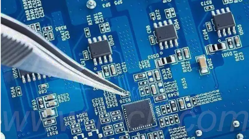
Antistatic Strategies
Antistatic protection plays an important role in the PCBA process because of the potential damage to sensitive electronic components caused by electrostatic discharge. Therefore, at the beginning of the PCB board design, it is necessary to fully consider and incorporate anti-static measures, so as to prevent damage to components caused by static electricity during the patch operation.
- Adopt anti-static material
PCB boards should be selected with anti-static function of the material or apply anti-static coating, which is particularly important in high-density and high-frequency circuit design. Common antistatic materials include antistatic paints and specific substrate materials. - Grounding Layout Planning
In the layout design of the PCB, the need for scientific and reasonable grounding layer to ensure that the static electricity in the circuit can be smoothly discharged. Grounding design not only helps to eliminate static electricity, but also effectively improve the anti-interference performance of the circuit.
Component selection and quality guidelines
① Component accuracy: all assembly bit number component type, model, nominal value and polarity marking should be strictly matched with the product assembly drawings and detailed list of requirements, the position of the placement is accurate.
② Component quality standards: components should be selected in line with the design specifications of the regular original products to ensure that they have excellent reliability, stability and excellent welding characteristics,to lay a solid foundation for the subsequent assembly process.
③ Thermal performance: for surface mount and assembly components,the metal electrodes and the package need to be able to withstand high temperature welding process temperature shock, there should be no damage,cracks,discolouration or deformation after welding and other undesirable phenomena.
Component mounting specifications
① Component positioning accuracy: components must be accurately aligned,the distance from the centre of the pad shall not exceed 1/4 of the size of the soldered end of the component. 3/4 of the width of the pins of the devices such as SOP, SOJ, QFP, PLCC, etc. shall be placed on the pad, and the toe and heel ends of the pins shall be adhered to the pad.
② placement pressure control: placement pressure (or height) should be adjusted to the appropriate range, to ensure that the components of the solder end or pin at least 1/2 of the thickness of the immersion of the solder paste. Too little or too much pressure may lead to poor soldering results.
③ Component layout planning: the layout and arrangement of components should follow the layout and direction of small components in front, to avoid blocking each other’s principles, and based on the layout of the circuit module, so that the relevant circuits with the same function constitutes a module, in order to facilitate the assembly and testing.
Heat resistance and material quality
In the PCBA chip processing process, PCB boards need to go through a number of heating processes, especially in the reflow soldering process, PCB must have excellent high temperature resistance. Therefore, the material of the PCB board and its thermal stability has become one of the core requirements in the chip processing.
- Material glass transition temperature (TG)
The glass transition temperature (TG) of PCB materials is an important indicator of their high temperature resistance. Generally speaking, the reflow soldering temperature can reach 250 ℃, which requires PCB board TG value should be located in the range of 130 ℃ to 170 ℃. For the need to operate in a high-temperature environment for electronic products, such as automotive electronics, PCB materials, the TG value of the more stringent requirements to ensure the reliability of its long-term operation. - Laminated structure of the stability of the
For multi-layer PCB boards,in the SMD process to ensure that the bonding strength between the layers is sufficient to prevent delamination at high temperature welding. The quality of the laminated material has a direct impact on the mechanical and electrical properties of the PCB board.
PCBA chip processing on the PCB board requirements are comprehensive and strict, involving welding, anti-static, component selection and placement, heat resistance and other dimensions. These requirements work together to ensure the quality and performance of the product, is an indispensable key link in the manufacture of electronic products.
