In a 4 layer PCB board, although signal crossing over reference plane gaps may seem minor, it can trigger a series of issues such as signal distortion, electromagnetic interference (EMI), and timing skew, compromising product stability and reliability.
Signal reflection is one of the most immediate consequences. When crossing gaps, impedance changes abruptly, preventing some signals from transmitting normally and reflecting them back to the source. This leads to signal distortion and degradation, affecting the overall operational stability of the PCB board.
The superposition of reflected and forward signals can also generate standing waves, further exacerbating signal interference. Particularly for high-frequency signals, which travel rapidly in 4 layer PCB board, reflection issues caused by gaps are more pronounced, easily leading to data transmission errors.
Increased crosstalk is another significant hazard. Reference plane gaps undermine the isolation between signals, allowing adjacent signal lines to suffer from mutual interference due to stray noise. This affects the normal operation of sensitive components and triggers functional abnormalities.
For high speed signals commonly used in 4 layer pcb boards, crosstalk issues become more pronounced. For instance, signals such as serial ports and SPI may experience misjudgment due to excessive crosstalk, causing confusion in the PCB board’s control logic and even leading to device crashes or restarts.
EMI radiation exceeding standards is a consequence that is often overlooked but poses significant harm. When signals detour around gaps, the loop area increases, effectively creating an “electromagnetic radiation source” that exceeds industry EMC standards.
Excessive EMI radiation not only affects the performance of the PCB board itself but also interferes with surrounding electronic devices. This can result in the product failing electromagnetic compatibility tests, increasing rectification costs, delaying mass production delivery timelines, and damaging the company’s reputation.
Timing skew is also a common issue. When signals detour around gaps, the increased travel distance leads to longer transmission delays, disrupting the original timing design and causing signal synchronization abnormalities. Especially in high-speed PCB boards, timing deviations can directly lead to functional failures.
Timing skew also reduces signal transmission rates. 4 layer PCB board are often used in mid-to-high-end electronic devices that demand high signal rates. Timing issues caused by gaps limit the performance ceiling of the PCB board, preventing it from meeting high-end requirements.
Increased power consumption is another easily overlooked issue. Signal detours generate additional losses, raising the power consumption of the PCB board. This not only increases device energy consumption but also causes localized heating on the board, accelerating component aging and shortening product lifespan.
Severe localized heating can even pose safety hazards. In 4 layer PCB board, where the power plane and ground plane are adjacent, excessive heating near gaps can damage the insulating layer and even trigger short circuits, resulting in PCB board burnout and equipment damage.
The occurrence of reference plane gaps in 4 layer PCB board is primarily related to design and manufacturing processes. Unreasonable design and improper layout are the primary causes, such as excessive reference plane segmentation or improperly placed gaps, which lay the groundwork for subsequent issues.
Lapses in the manufacturing process can also create gaps. For example, insufficient precision in etching processes can lead to irregular gaps in the reference plane, while positioning deviations during lamination can result in poor reference plane alignment, forming hidden gaps.
To avoid these issues, the design phase should optimize reference plane layout. Minimize reference plane segmentation and avoid placing gaps on signal transmission paths. If segmentation is necessary, implement proper gap-crossing measures to ensure unobstructed signal return paths.
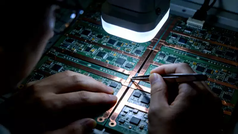
Gap-crossing measures can include bridge designs, such as placing sufficiently wide copper foil bridges at gaps to shorten signal detour distances. Alternatively, star or single-point grounding methods can be employed to reduce the impact of gaps on signal transmission.
The manufacturing process should enhance precision control. Strictly control tolerances in etching processes to prevent gaps in the reference plane. Before lamination, ensure proper positioning and alignment to guarantee tight reference plane connections and eliminate hidden gaps.
Testing and verification serve as the final line of defense. Conduct signal integrity and EMI tests on 4 layer PCB board before mass production to identify and rectify issues caused by reference plane gaps, preventing non-compliant products from entering downstream processes.
Many PCB companies fall into the cognitive trap of believing that reference plane gaps are “insignificant and harmless,” neglecting design and manufacturing controls. In reality, in 4 layer PCB board, these hidden hazards are amplified, and the cost of late-stage rectification far exceeds early-stage prevention.
Especially in high-end fields such as automotive electronics and industrial control, where 4 layer PCB boards demand extremely high stability, issues caused by signal crossing reference plane gaps can lead to equipment failures and even safety accidents.
As the application of 4 layer PCB boards becomes increasingly widespread, signal integrity and electromagnetic compatibility have become core competitiveness. Only by avoiding reference plane gap hazards can PCB board quality be ensured and product market acceptance be improved.
In summary, although signal crossing over reference plane gaps in 4 layer PCB boards may seem minor, they pose significant hazards that directly impact signal integrity, EMI compliance, and product reliability. Only through design optimization and manufacturing process control can risks be mitigated at the source.
