A PCB is a functional board that provides point-to-point connection of wires and printed components on an insulated substrate, according to a predetermined design.A PWB is a functional board that provides point-to-point connection of wires on an insulated substrate, according to a predetermined design, but does not contain printed components.
PWBs, or printed wiring boards, were the substrates for early electronic devices and were characterized by the absence of circuit diagrams and printed components, but rather by the use of an epoxy glass substrate and the formation of connections through an etching process to achieve conductive insulation between the wires. This technology emphasizes the function as a carrier for carrying components, and generates electronic circuits by manually drawing and etching circuits to achieve point-to-point component connections.
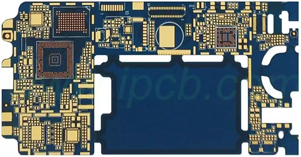
PCB Chinese name for printed circuit boards, also known as printed circuit boards, is an important electronic components, is the support body of electronic components and electronic components electrical connection carrier. Because it is the use of electronic printing technology, so it is called “printed” circuit boards. PCB is used in almost all electronic products, is an indispensable electronic component of modern electronic information products, known as “the mother of electronic products”.
The difference between PWB vs PCB: the former already contains components that constitute the circuit function, the latter only plays a conductive role in connecting the line. The difference lies in whether it contains printed components,circuit board can contain wiring board,and PWB can not be equated with PCB. international standard IEC 60194-22017, national standard GB/T 2036-1994 and the industry group standard CPCA 1001-2022 have on the PCB and PWB definition. Definition. In the above standards, PCB and PWB are collectively referred to as printed board (PB), indicating the relationship between the two.
Differences in Manufacturing Processes
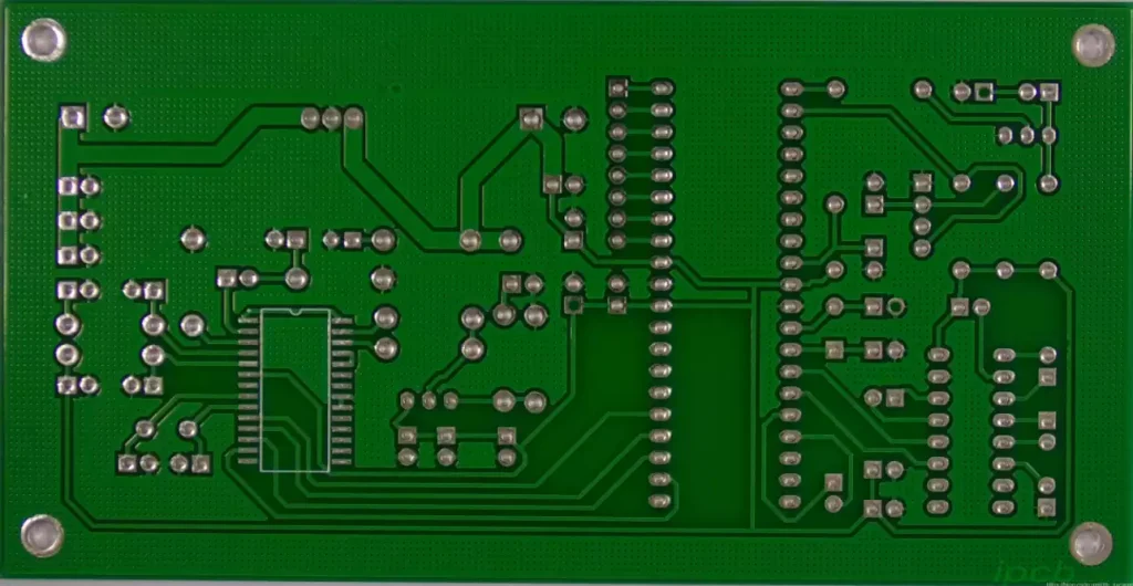
The manufacturing process of PWB is relatively simple, mainly through the inkjet printing method on the substrate sprayed with conductive ink, so that the circuit signals can be transmitted. Usually white, green and other colors of the substrate, only one side of the printed circuit, generally used for some simple circuit board connections, such as lithium battery protection board.
PCBs, on the other hand, are manufactured through a series of complex processes such as laminating the substrate with copper foil and etching and chemically plating the copper foil. High-precision circuits need to be fabricated through complex processes such as photolithography and gold plating. Therefore, PCB is higher than PWB in terms of production cost and manufacturing difficulty, and is suitable for industrial, communication electronics and other fields.
Differences in application scenarios
Due to the different production processes, PWB and PCB are also different in application scenarios. Generally speaking, PWB is suitable for the production of some simple circuits, mainly used for a small amount of handmade, such as DIY enthusiasts to make their own cell phone battery protection boards, LED strips and so on.
PCB, on the other hand, is suitable for mass production because of its lower manufacturing cost and higher efficiency, and is widely used in wireless communications, computers, consumer electronics and other fields.
As key components in the electronics industry, PWB vs PCB each have unique characteristics and application scenarios. With the continuous development of science and technology, both will continue to play an important role in their respective fields and jointly promote the progress of the electronics industry. In the future, we expect these two technologies to continue to innovate and improve, injecting new vitality into the development of electronic products.