In the manufacture of RF and microwave circuits, Rogers PCBs serve as the core substrate due to their low dielectric loss and high dielectric stability. As the critical process for connecting components to the PCB, the soldering process directly determines the product’s signal integrity and long-term reliability. Unlike conventional FR4 boards, the special materials used in Rogers PCBs—such as hydrocarbon-filled ceramics and PTFE-based composites—place higher demands on soldering temperature, solder selection and pad preparation. Even the slightest oversight during the soldering process can lead to issues such as cold solder joints, pad detachment and compromised dielectric properties.
Many PCB manufacturers in the industry still rely on traditional FR4 soldering experience when handling Rogers PCBs, ultimately resulting in low product yield rates. A soldering process truly suited to Rogers PCBs requires a comprehensive understanding of the board’s physical properties and component types, with strict control throughout the entire process from initial design to final soldering; this is also the core competitive advantage in the mass production of high-end RF products.
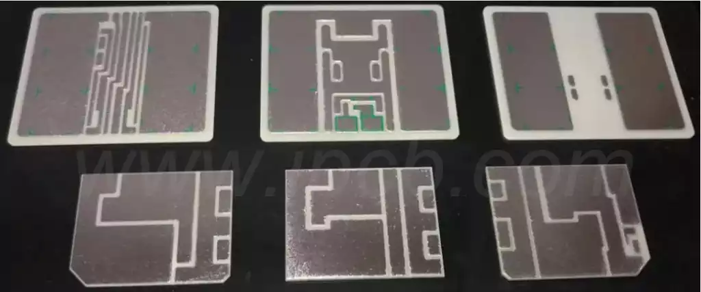
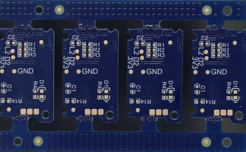
Pad Design
The structural and dimensional design of pads is the most fundamental yet critical aspect of the Rogers PCB soldering process. An inappropriate pad design can directly cause soldering defects and even compromise the board’s high-frequency performance. The dielectric layers of Rogers PCBs are predominantly made of materials with a low coefficient of thermal expansion, which differs significantly from that of copper foil. This necessitates that pad design must balance both soldering reliability and board stability.
For RF signal pads, in addition to meeting standard impedance matching requirements, post-soldering electrical performance must also be considered. In high-frequency soldering scenarios for Rogers PCBs, pad edges should feature a rounded transition design to avoid electric field concentration caused by right-angled structures, thereby reducing signal reflection and loss. Additionally, the copper foil thickness of the pads must be matched to the board thickness; the recommended copper foil thickness for standard Rogers PCB pads is 1 oz to 2 oz. Excessively thick copper foil can hinder heat conduction during soldering, whilst excessively thin foil is prone to deformation during the process.
In actual production, attention must also be paid to the treatment of the solder mask during the design of Rogers PCB pads. The thermal expansion coefficient of the solder mask ink differs significantly from that of the Rogers PCB substrate. If the solder mask around the pad is too thick, thermal stress during soldering may cause the solder mask to crack, thereby affecting the adhesion of the pad.
It is recommended to create a window in the solder mask within a 0.5 mm radius of the pad, ensuring the distance between the edge of the window and the pad edge is maintained at 0.1 mm or more. This ensures sufficient space for soldering operations whilst minimising the impact of thermal stress on the board.
For the pad design of packaged components such as BGAs and QFNs, Rogers PCBs must utilise ball-padded or stepped pad structures to prevent cold solder joints caused by insufficient pad flatness. Additionally, pad spacing must be adjusted according to the soldering process. There are differences in pad spacing between wave soldering and reflow soldering; wave soldering requires larger gaps between pads to prevent solder bridging, whilst reflow soldering allows for slightly smaller gaps to increase soldering density.
Pre-soldering Treatment
Pre-soldering treatment is a critical step in eliminating soldering defects in Rogers PCBs, comprising two key processes: board cleaning and pad activation. Surface treatment processes for Rogers PCBs typically include electroless gold plating, OSP and tin plating; the pre-soldering treatment requirements vary depending on the surface treatment method, and improper treatment can directly affect solder wettability.
For Rogers PCBs with an electroless gold finish, the degreasing and activation processes must be strictly controlled prior to soldering. The nickel layer within the electroless gold plating is prone to oxidation, and the resulting oxide layer severely impedes the bonding between the solder and the copper foil. Therefore, a weakly acidic activator must be used for treatment, with the processing time strictly limited to within 30 seconds to avoid excessive corrosion of the nickel layer. In actual production, many manufacturers omit the activation step to simplify the process; this is one of the primary causes of cold solder joints in Rogers PCBs.
For Rogers PCBs with OSP surface treatment, the core of pre-soldering preparation is the removal of the organic protective film from the surface. As the dielectric properties of Rogers PCBs are sensitive to chemical reagents, the use of strongly alkaline degreasing agents is strictly prohibited. Neutral or weakly acidic degreasing solutions must be selected, and the PCB must be thoroughly rinsed with deionised water after treatment to prevent residual chemicals from affecting soldering quality.
Furthermore, Rogers PCBs must undergo drying treatment prior to soldering, with the temperature controlled between 80°C and 100°C and a drying time of no less than 30 minutes. This removes moisture from the board to prevent bubbling at the pads caused by moisture vaporisation during soldering.
For high-frequency signal pads, pre-soldering treatment must also avoid excessive polishing. The surface roughness of the copper foil on Rogers PCBs affects signal transmission loss; excessive polishing damages the original structure of the copper foil, increasing signal loss. Only pads with severe oxidation require light polishing.
Soldering Parameters
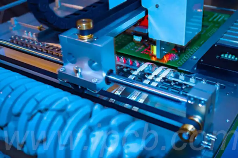
Precise control of soldering parameters is key to the success of high-frequency soldering on Rogers PCBs. The unique composition of Rogers PCBs makes them highly sensitive to parameters such as temperature, time and solder; incorrect parameter settings can lead to issues such as poor solder wetting, thermal damage to the board and changes in dielectric constant.
Reflow soldering is the most commonly used process for Rogers PCBs, and the temperature profile must be tailored to the specific board type. For Rogers RO4000 series ceramic-filled hydrocarbon boards, the peak temperature during reflow soldering should be maintained between 245°C and 255°C, with a dwell time above the liquidus line of 30 to 60 seconds to prevent thermal ageing of the board caused by prolonged exposure to high temperatures. Conversely, for PTFE-based Rogers RT/Duroid series boards, the peak temperature should be reduced to 235°C–245°C, with the dwell time shortened to 20–40 seconds, to prevent the decomposition of the PTFE material at high temperatures.
Soldering speed is also a critical parameter affecting the quality of Rogers PCB soldering. Excessively high soldering speeds can result in inadequate solder wetting and cold solder joints; whereas too slow a rate increases thermal stress, leading to pad deformation. In actual production, it is recommended to adjust the soldering speed according to component size: for small surface-mount components, the soldering speed should be controlled at 0.8–1.2 m/min, whilst for large BGA components, it should be reduced to 0.5–0.8 m/min to ensure adequate solder wetting.
The choice of solder is equally critical. For high-frequency soldering of Rogers PCBs, lead-free solder is the preferred option. We recommend Sn99.3Cu0.7 or Sn96.5Ag3.0Cu0.5 solder wire or paste, as these have a moderate melting point, good wettability, and meet environmental requirements. The use of leaded solder should be avoided, as it not only fails to meet industry environmental standards but may also cause thermal damage to Rogers PCB boards due to the solder’s excessively high melting point.
Furthermore, the control of the nitrogen atmosphere during the soldering process must not be overlooked. In high-frequency soldering of Rogers PCBs, a nitrogen atmosphere effectively reduces solder oxidation and improves wettability. Nitrogen purity must be maintained at 99.99% or higher, with oxygen content below 100 ppm; particularly for the soldering of fine-pitch components, a nitrogen atmosphere is a prerequisite for ensuring soldering quality.
Defect Management
Common defects in Rogers PCB soldering production include cold solder joints, solder bridging, pad detachment and board blistering. Targeted corrective measures must be implemented for different defects, whilst process optimisation is required to reduce defect rates.
Cold solder joints are the most common defect in Rogers PCB soldering, primarily caused by pad oxidation, poor solder wettability and insufficient soldering temperature. When addressing this issue, the first step is to verify whether pre-soldering activation has been carried out correctly; for severely oxidised pads, the activation process must be repeated.
If the soldering temperature is insufficient, the reflow soldering temperature profile should be adjusted to appropriately increase the peak temperature. For cold solder joints in fine-pitch components, a hot-air rework station can be used for re-soldering; during rework, temperature and time must be carefully controlled to avoid secondary damage to the board.
Solder bridging frequently occurs between fine-pitch pads, primarily due to excessive solder paste deposition and insufficient pad spacing. To address this, the solder paste printing process must be optimised by adjusting the stencil thickness and aperture size to ensure precise solder paste application; for joints where bridging has already occurred, use a hot-air rework station in conjunction with desoldering tape for cleaning, taking care to avoid prolonged exposure to high temperatures during the process.
Pad delamination is a relatively serious defect in the soldering of Rogers PCBs, primarily caused by excessive thermal stress and insufficient adhesion of the pad copper foil. Preventive measures include optimising pad design, controlling the soldering temperature profile, and adopting a stepped pad structure; if pad delamination occurs, it can be addressed by fly-wire repair or remanufacturing the pads. Following repair, the board must undergo thermal stability testing to ensure that dielectric properties remain unaffected.
Bubbling of the board typically occurs under high soldering temperatures and is mainly caused by internal moisture or residual solvents. To address this, the pre-soldering drying process must be enhanced, and the humidity of the board’s storage environment must be strictly controlled; boards that have already developed bubbles must be scrapped to prevent any impact on product performance.
Post-Soldering Inspection and Validation
Inspection and validation following the completion of soldering constitute the final stage of the Rogers PCB soldering process and are a crucial safeguard for ensuring product quality. As high-frequency substrates,Rogers PCBs require not only routine visual inspections but also electrical performance and reliability testing to comprehensively validate soldering quality.
Visual inspection primarily checks the wettability and integrity of solder joints, looking for defects such as cold solder joints, bridging, or pad detachment; an optical microscope may be used to inspect fine-pitch solder joints. For RF signal solder joints, the flatness of the pads must also be checked to prevent raised solder joints from affecting signal transmission.
Electrical performance testing focuses on high-frequency signal pads, utilising a vector network analyser to measure parameters such as impedance matching, insertion loss and return loss, thereby verifying whether the post-soldering dielectric properties meet design requirements. Should any abnormal parameters be detected, the soldering process must be investigated for potential issues, such as unreasonable pad design or excessive soldering temperatures causing changes in the dielectric constant.
Reliability testing includes thermal shock testing, temperature and humidity storage testing, and vibration testing, which simulate operating conditions in the product’s actual usage environment to verify the long-term reliability of the solder joints. As Rogers PCBs have a low coefficient of thermal expansion, the recommended temperature range for thermal shock testing is -40°C to 125°C, with a minimum of 500 cycles; the integrity of the solder joints and pads must be inspected following the test.
The soldering process for Rogers PCBs is, in essence, a process of deep adaptation to the material’s properties. From pad design to post-soldering inspection, every stage requires moving away from the conventional practices associated with FR4 and returning to precise control over special materials such as ceramic-filled and PTFE substrates.