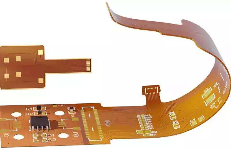
Flexible printed circuits, with their exceptional flexibility and lightweight, slim form factor, seamlessly integrate into the intricate internal structures of various precision electronic devices. They have become a pivotal element driving the advancement of electronic equipment towards multifunctional integration and extreme miniaturisation.
Within the structural framework of flexible printed circuits, copper foil occupies a pivotal position, serving as the ‘core conductor’ for electrical transmission. It functions as the circuit board’s ‘nervous system’, undertaking the vital mission of efficient current and signal transmission. The quality standards and performance characteristics of copper foil directly influence core metrics of flexible circuit boards, including electrical conductivity, mechanical stability, and thermal dissipation efficiency. Consequently, it profoundly impacts the operational stability, service life, and user experience of electronic products. It is no exaggeration to state that the precise selection of copper foil constitutes a vital cornerstone in establishing the high quality of electronic products. So, how should one scientifically and rationally select copper foil for flexible circuit boards? We shall now delve into this matter in depth.
Classification and Characteristics of Copper Foil Manufacturing Processes
Rolled Copper Foil (RA Copper Foil)
As its name suggests, rolled copper foil is produced by repeatedly rolling high-purity copper ingots through multiple passes. This process resembles a master baker repeatedly rolling dough, ultimately creating a sheet as thin as gauze. During rolling, the ingot gradually thins under sustained pressure, resulting in a denser, more uniform crystalline structure. Once the target thickness is achieved, the foil undergoes surface treatments—such as precision roughening and oxidation resistance enhancement—tailored to specific applications, further optimising its performance.
This distinctive manufacturing process endows rolled copper foil with numerous exceptional properties. Firstly, it possesses remarkable ductility, akin to a rubber band, capable of withstanding significant bending and stretching without fracturing. This characteristic ensures that flexible circuit boards incorporating rolled copper foil maintain excellent conductivity even under frequent bending, providing stable and reliable signal transmission for the moving components of electronic devices. For instance, within the hinge mechanism of foldable smartphones, rolled copper foil flexes seamlessly with repeated screen openings and closings, ensuring uninterrupted current supply and maintaining device functionality. Secondly, rolled copper foil boasts an exceptionally smooth, mirror-like surface finish. This not only enhances product aesthetics but, more critically, offers significant advantages in high-frequency circuit applications. During high-speed signal transmission, this flawless surface drastically reduces signal reflection and loss, guaranteeing signal integrity. This enables data to travel rapidly and accurately, akin to vehicles (signals) traversing an unobstructed motorway. In demanding applications such as high-end communication base stations and precision medical monitoring equipment, where signal transmission quality is critically important, rolled copper foil excels, supporting the precise operation of such devices.
Electrolytic Copper Foil (ED Copper Foil)
The production of electrolytic copper foil resembles a “marvellous journey of electrodeposition” within the microscopic realm. First, copper material is dissolved in a specific electrolyte to create a solution rich in copper ions. At this stage, these copper ions act like “little sentinels” awaiting their call to action. Next, specially treated stainless steel cathode rolls and anode plates are placed within the electrolytic cell, with direct current applied. Under the influence of the electric field, the copper ions respond as if to a clarion call, rapidly migrating towards the cathode roll. There, they acquire electrons, reverting to copper atoms that deposit layer by layer, much like forging a copper ‘armour’ over the cathode roll. As deposition progresses, the copper layer gradually thickens to the required specification. It is then gently peeled from the cathode roll. Following subsequent cleaning, drying, and surface treatment processes, the electrolytic copper foil is complete.
The significant advantage of electrolytic copper foil lies in its relatively low cost and high production efficiency. Owing to the simplicity of the electrolytic process, it lends itself readily to large-scale industrial production, enabling rapid fulfilment of substantial market demand for copper foil. Consequently, it finds widespread application in the manufacture of circuit boards for numerous commonplace electronic products. Examples include standard computer motherboards and household appliance control circuit boards. These products are cost-sensitive and involve relatively infrequent bending of the circuit boards. Electrolytic copper foil ensures fundamental electrical conductivity while effectively controlling costs. However, electrolytic copper foil is not without its limitations. Its columnar crystal structure renders it less resilient to bending forces than rolled copper foil, making it more prone to fracture. This is analogous to bending tests conducted on wooden sticks and bamboo of identical thickness, where the columnar structure within bamboo makes it more susceptible to breaking. Consequently, in areas of flexible circuit boards requiring frequent bending and demanding exceptional flexibility, electrolytic copper foil proves inadequate.
Selection Strategy for Copper Foil Thickness
Copper foil constitutes the conductive layer bonded to an insulating substrate, which is subsequently etched selectively to form conductive circuits. The vast majority of this foil utilises either rolled copper foil or electrolytic copper foil. Rolled copper foil exhibits superior ductility and bending resistance compared to electrolytic copper foil, with elongation rates ranging from 20% to 45% for rolled foil versus 4% to 40% for electrolytic foil. The most commonly used copper foil thickness is 35μm (1oz), though thinner 18μm (0.5oz) or thicker 70μm (2oz) foils are also available, extending up to 105μm (3oz). The appropriate copper foil type must be selected based on specific application requirements. Where the sole purpose is to replace wires and connectors, thereby reducing manufacturing time and costs, electrolytic copper foil—well-suited for flexible printed circuits—constitutes the optimal choice. Electrolytic copper foil is also employed where increased copper mass enhances current-carrying capacity, enabling achievable copper strip widths.
Within flexible circuit board design, selecting copper foil thickness constitutes a highly nuanced discipline, requiring comprehensive consideration of multiple factors to achieve optimal balance.
On one hand, copper foil thickness is determined by the minimum lead width and minimum spacing. This is analogous to bridge construction: the deck width (corresponding to lead width) and the span between piers (corresponding to lead spacing) dictate the appropriate building material specification (i.e., copper foil thickness). Generally, thinner copper foil enables smaller minimum lead widths and spacings. This is of paramount importance for electronic products striving for extreme miniaturisation and precision. For instance, in high-end micro-medical implant devices and ultra-compact sensors, thinner copper foil—such as 9μm, 12μm, or even finer specifications—is essential to accommodate more complex circuitry within limited space, thereby enabling greater functionality. Only through such precision can intricate circuit designs be realised, ensuring flawless device operation and providing robust support for medical diagnostics, environmental monitoring, and similar applications.
Conversely, varying copper foil thicknesses significantly impact a circuit board’s conductivity, mechanical properties, and thermal conductivity. Thicker foils, such as those at 35μm and above, function like broad, unobstructed ‘highways,’ capable of carrying greater currents with relatively lower resistance. In high-current applications, thick copper foil effectively reduces circuit heating, ensuring stable operation. In equipment such as high-power power supply modules and electric vehicle control systems, where substantial currents flow during operation, thick copper foil fully leverages its advantages to ensure reliable device performance and prevent faults caused by circuit overheating. However, thick copper foil also possesses inherent limitations. Due to its considerable weight and poor flexibility, it is unsuitable for areas requiring frequent bending. Forcing such bends can readily cause the foil to fracture, resulting in circuit interruptions. In stark contrast, thin copper foil, while possessing relatively lower current-carrying capacity, offers exceptional flexibility. It readily accommodates repeated bending, much like a supple ribbon. In areas requiring bending within flexible circuit boards—such as the folding hinges of foldable smartphones or the articulated joints of wearable devices—thin copper foil ensures continuous and stable signal transmission, thereby guaranteeing proper device functionality.
Selecting copper foil for flexible circuit boards involves a complex process that comprehensively evaluates multiple factors, including manufacturing processes and thickness. A balanced consideration of process requirements and thickness, tailored to specific product needs, is essential to ensure performance and support the stable development of electronic devices.