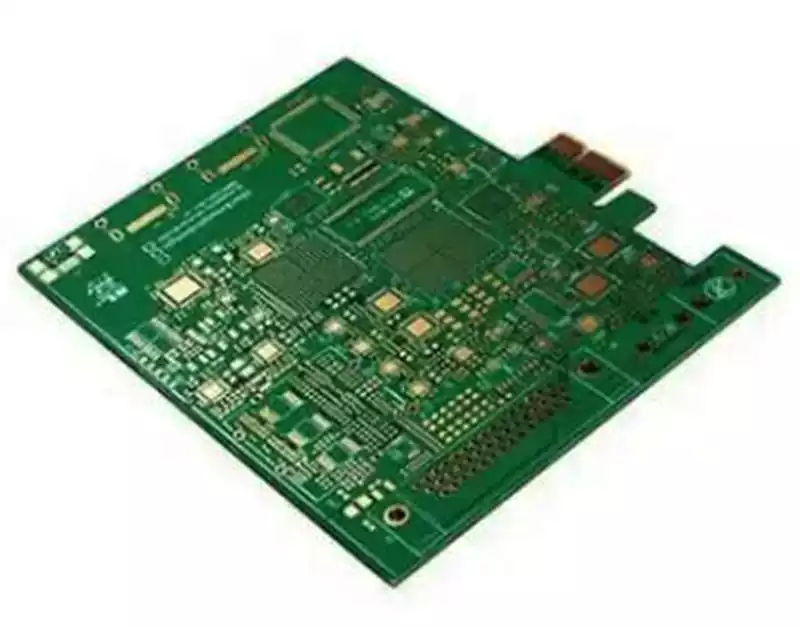
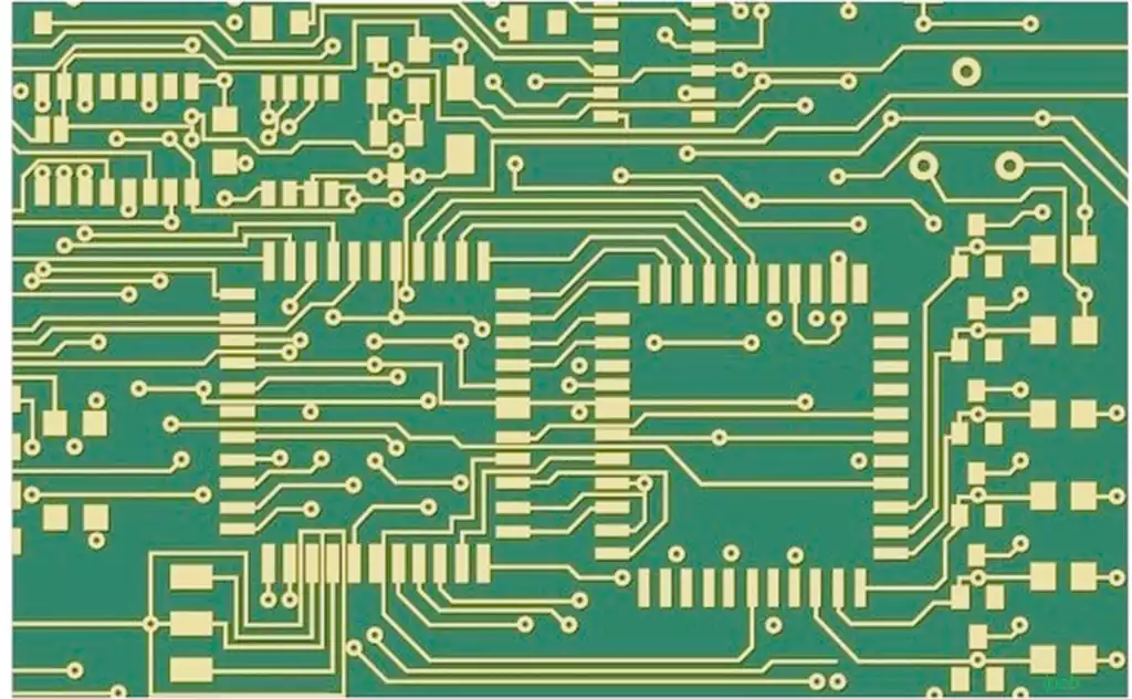
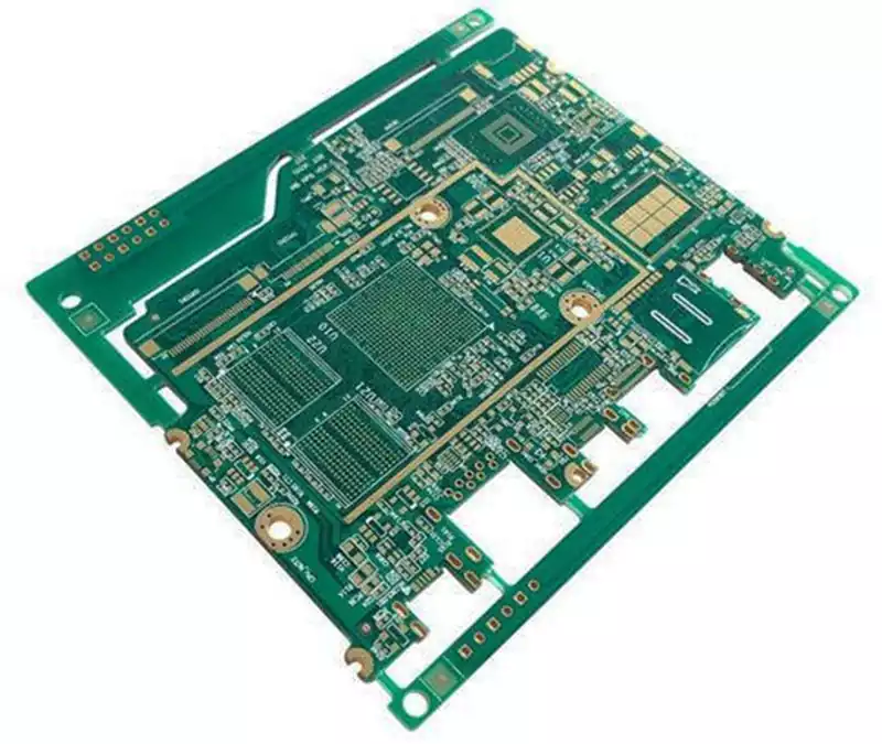
As the most widely used substrate material, the glass fibre epoxy structure of FR4 PCBs inherently predisposes their surface copper layers to oxidation and poor solderability. The three mainstream surface finishing processes—HASL, ENIG, and OSP—function like distinct protective armour for FR4 PCBs, each tailored to different application scenarios and performance requirements.
Selecting the appropriate process is never a simple matter of determining which is ‘more advanced.’ Rather, it requires a comprehensive decision-making process that balances the FR4 PCB’s cost budget, soldering requirements, operating environment, and product lifespan. Only by thoroughly analysing the compatibility logic of these three processes can the performance of FR4 PCBs be maximised.
The core objective of FR4 PCB surface finishing is to protect exposed copper traces—mitigating oxidation—while ensuring reliable solderability and stable electrical performance. In ambient conditions, copper layers on FR4 substrates readily oxidize, and the resulting copper oxides significantly degrade solder joint quality, leading to defects such as cold solder joints or pad lift. Under complex service conditions, factors such as salt spray, humidity fluctuations, and thermal cycling further accelerate corrosion of the PCB, shortening its service life.
Surface finishes are designed to address these challenges. On the one hand, they form a dense protective barrier that isolates copper from air and moisture, slowing oxidation and corrosion; on the other hand, they provide a solderable interface that ensures robust metallurgical bonding between component leads and PCB traces. Because different surface-finish processes vary significantly in protection mechanisms, layer structures, and performance characteristics, their suitability for FR4 applications also differs. This fundamental diversity explains why no single process can universally satisfy all FR4 PCB requirements.
HASL (Hot Air Solder Leveling), ENIG (Electroless Nickel/Immersion Gold), and OSP (Organic Solderability Preservatives) each emphasize different strengths in terms of process principles, complexity, and performance, resulting in distinct compatibility profiles with FR4 PCBs. Only by understanding the intrinsic nature of each process can their appropriate application boundaries be clearly defined.
HASL: A Traditional and Cost-Effective Choice
HASL is one of the oldest PCB surface-finish technologies. The process involves immersing the FR4 PCB into molten solder—traditionally tin-lead, now more commonly lead-free tin alloys—followed by hot air leveling to remove excess solder and form a coating on the copper surface. Its compatibility with FR4 stems from its mature process logic and stable protective performance.
Key advantages for FR4 include three aspects. First, controllable cost: HASL features simple processing steps and high throughput without complex chemical treatments, with a unit-area cost typically only one-third to one-half that of ENIG, making it highly attractive for high-volume, cost-sensitive FR4 PCBs such as consumer electronics power boards or home-appliance control boards. Second, excellent solderability: the tin-based alloy layer bonds well with component leads, forming reliable intermetallic compounds and achieving high soldering yields. Third, process maturity and robustness: HASL places relatively low demands on FR4 material properties—whether standard Tg or high-Tg FR4—and delivers stable yields with a low technical barrier.
However, HASL also presents clear limitations. First, poor surface flatness: during hot air leveling, solder thickness can be uneven, with surface roughness reaching 5–10 μm, making it unsuitable for fine-pitch components (e.g., QFP packages with pitches below 0.4 mm) due to solder paste printing nonuniformity and increased short-circuit risk. Second, challenges in lead-free implementation: traditional leaded HASL no longer meets environmental regulations, while lead-free HASL requires higher soldering temperatures (often above 260 °C), which can stress low-Tg FR4 substrates (Tg ≤130 °C) and cause warpage. Third, limited edge protection: solder thickness at board edges is often thinner, making HASL-finished FR4 PCBs more susceptible to edge corrosion in humid or salt-spray environments, thus unsuitable for outdoor or harsh conditions.
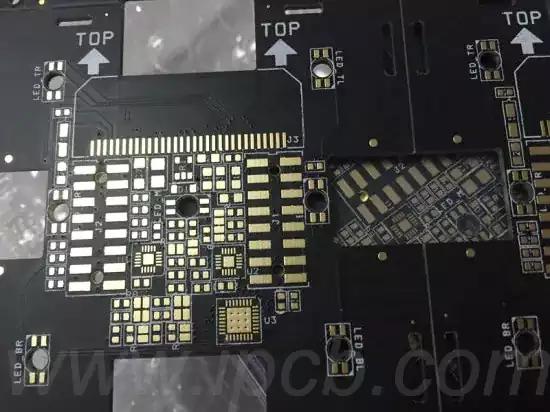
ENIG: A High-End, Precision-Driven Performer
ENIG is the dominant surface-finish technology for high-end FR4 PCBs. The process deposits a nickel-phosphorus alloy layer onto the copper surface via electroless plating, followed by a thin immersion gold layer, forming a dual-layer structure of “nickel foundation with gold protection.” This configuration aligns ENIG with high-precision, high-reliability FR4 applications.
Its advantages are pronounced. First, exceptional surface flatness: chemical deposition allows precise thickness control, achieving surface roughness of 1–2 μm, ideal for fine-pitch and high-density FR4 PCBs such as smartphone motherboards and precision industrial control boards. Second, superior corrosion protection: gold’s chemical stability effectively blocks air and moisture, while the nickel layer further inhibits corrosion penetration, extending PCB service life by three to five times in humid, salt-spray, or high-temperature environments—well suited for outdoor equipment and medical devices. Third, excellent electrical performance: the gold layer provides low contact resistance and uniform thickness, ensuring stable signal transmission for high-frequency FR4 PCBs such as those used in 5G communications. Fourth, strong resistance to multiple reflow cycles: ENIG coatings can typically withstand three to five 260 °C reflow cycles without oxidation, accommodating complex assembly processes.
ENIG’s drawbacks are primarily cost and process complexity. Chemical plating chemicals are expensive, and the multi-step process—degreasing, micro-etching, activation, electroless nickel plating, and immersion gold plating—results in unit costs two to three times higher than HASL, limiting its economic feasibility for low- and mid-range FR4 PCBs. Additionally, improper process control can lead to the “black pad” phenomenon, where nickel oxidation at the nickel-gold interface causes solderability issues, demanding stringent process management. ENIG also requires high substrate cleanliness; surface contamination can compromise adhesion, increasing pre-treatment costs.
OSP: An Environmentally Friendly Solution for Fine-Pitch Designs
OSP is an eco-friendly surface-finish technology that forms an ultra-thin organic protective film (0.1–0.3 μm) on the FR4 copper surface through chemical adsorption. This film prevents oxidation during storage and volatilizes during soldering without impairing joint formation. Its lightweight protection mechanism makes it particularly suitable for environmentally conscious, fine-pitch FR4 applications.
OSP’s strengths include outstanding environmental compliance, as it contains no heavy metals and generates minimal wastewater, fully meeting RoHS and REACH requirements. Its extremely smooth surface—comparable to bare copper with roughness ≤1 μm—supports ultra-fine pitches below 0.3 mm and does not increase PCB thickness, making it ideal for thin and lightweight FR4 designs such as notebooks and wearable devices. Cost is moderate, with simpler processing steps than ENIG, offering a balance between performance and expense. Moreover, the low-temperature process (below 100 °C) minimizes thermal stress, making OSP suitable for low-Tg FR4 substrates.
Limitations include a relatively short protection window—typically three to six months under ambient conditions—and limited resistance to multiple reflow cycles, generally only one or two at 260 °C. OSP also provides minimal protection against salt spray or chemical corrosion, restricting its use in harsh environments, and requires precise soldering temperature control to ensure complete film decomposition.
Comparative Overview and Selection Guidelines
From a cost perspective: HASL < OSP < ENIG. HASL suits cost-sensitive FR4 PCBs; OSP fits value-oriented, fine-pitch mid-to-high-end designs; ENIG targets premium, reliability-critical applications. From flatness and fine-pitch compatibility: ENIG ≈ OSP > HASL.
From protection and service life: ENIG > HASL > OSP.
From environmental compliance and soldering requirements: OSP > ENIG > lead-free HASL.
A practical three-step approach helps determine the optimal surface finish. First, define the core requirement—cost minimization, fine-pitch with environmental compliance, or maximum reliability. Second, align with component pitch and soldering demands, excluding processes that cannot meet pitch or reflow requirements. Third, evaluate operating environment and lifespan expectations, selecting ENIG for harsh or long-life applications and HASL or OSP for benign indoor conditions.
As the electronics industry continues to advance toward thinner, more precise, and greener designs, the application scope of ENIG and OSP will expand, while HASL will remain relevant in cost-driven segments. Selecting the appropriate surface finish technology enables FR4 PCBs to fully realize their performance potential and ensures long-term, reliable operation of electronic products.