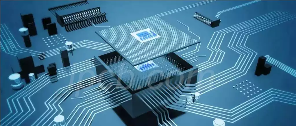
SIP (System in Package) and SOC (System on Chip) as two important trends in PCB design, their development not only affects the performance and size of the product, but also has a far-reaching impact on the future direction of the entire electronics industry.
SoC is System on Chip. From a narrow perspective, SoC is the chip integration of the core of the information system, which is the integration of key system components on a chip; from a broad perspective, SoC is a micro-small system. Compared with the general chip definition, SoC emphasizes more on a system as a whole, i.e., the combination of multiple integrated circuits with specific functions on a single chip, the technology of overall design and processing of all or part of the necessary electronic circuits, and ultimately the formation of a system or product containing complete hardware and software.
SoC system-on-chip chip has its advantages in many aspects, the main performance:
- Light weight, small size, strong portable performance. As a result of the integration of multiple function module ICs into one SoC, the package size can be effectively reduced, and the application can effectively reduce the area occupied by the PCB;
- Low power consumption, fast operation speed, and strong low latency performance. Multiple function module signals to achieve internal transmission, the distance is greatly reduced, not only to reduce power consumption, while the signal transmission efficiency is improved, thus improving product performance;
- On the same area of silicon, SoC has efficient system integration capability and enriches system functions;
- SoC system-on-chip chips are integrated into a single wafer, with the same thermal effect, electromagnetic compatibility characteristics have been greatly improved, the overall performance of the chip has been improved;
- Mass production can provide the lowest cost of the realized function.
Because SoC has an unprecedented high efficiency integration performance, and in power consumption, reliability, and the scope of application have obvious advantages, at present in the performance and power sensitive terminal chip field, SoC has occupied a dominant position, and its application areas are expanding, it is the main solution to replace the decentralized multi-module integrated circuits.
Nevertheless, there are still some problems to be solved in SoC:
- SoC development is actually a combination of IP modules, due to the progressive increase in the complexity of the chip structure, which may lead to increased test costs, test cycle is greatly extended, the production yield is reduced, and the cost of a single product is high;
- SoC system-on-chip complexity increases, so the risk of design errors, product delays, and chip manufacturing iterations leading to increased costs is high, and time-to-market is long;
- SoC system-on-chip technology integrates digital, analog, RF, microwave signals, MEMS, etc. on the same chip with process compatibility issues.
The problems encountered in the development of SoC system-on-chip chips can be remedied to a greater extent by advanced packaging technologies, i.e., MCM packaging technology and SIP system-in-package (SIP) technology.
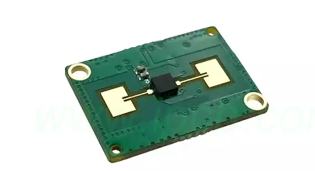
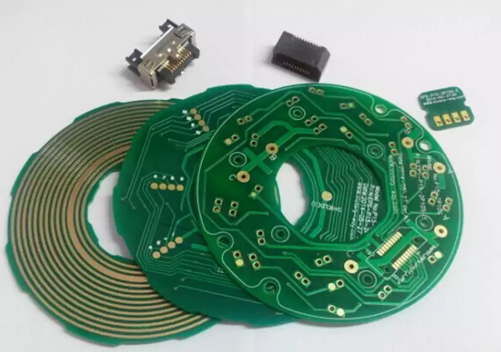
SIP (System In Package) is a packaging concept that takes multiple semiconductors and some necessary auxiliary parts and makes them into a relatively independent product that can realize certain system-level functions and encapsulates them in a shell. Eventually in the form of a part in the higher-order system-level PCBA (Printed Circuit Board Assembly).
Due to the use of different interconnect processes such as flip-flop, it can be categorized into FC-SiP and FC/WB-SiP, etc. SiP containing chips stacked vertically is called 3D SiP.
System-in-Package (SIP) technology from the early 1990s to the present, after more than a decade of development, has been able to be widely accepted by academia and industry, and has become one of the new hotspots of electronic technology research and the main direction of technology application.
And that he represents the direction of future development of electronic technology, SIP packaging process as an important part of the SIP packaging technology.
SiP Package Advantages
In the field of IC packaging, it is an advanced package with rich connotations and outstanding advantages, and there have been a number of important breakthroughs, the architecture of the chip plane placed in the stacked package, so that the density increases, the performance is greatly improved, on behalf of the development trend of the Phoenix technology, there are great advantages in a variety of aspects of the characteristics, as reflected in the following aspects.
(1) SiP realization is the integration of the system. To be given to the package body to complete a system target product all interconnections as well as functionality and performance parameters, can be utilized at the same time the lead bonding and flip-solder interconnect technology and other IC chip stacking and other direct interconnect technology, multiple IC chips and discrete active and passive devices encapsulated in a tube shell.
(2) Increase the package area, SiP in the same package kind of stacked two or more chips. The vertical direction of the space to use up, while not having to increase the pin-out, chip stacked in the same shell, the overall package area is greatly reduced.
(3) The use of ultra-thin chip stacking and TSV technology makes the multi-layer chip stacking package volume reduction, the most advanced packaging technology can be realized in multi-layer chip stacking thickness.
(4) SiP can be different materials, compatible with different GaAs, Si, InP, SiC, ceramics, PCB and other materials for the combination of integrated packaging.
(5) All components in a package shell, shorten the circuit connection, see a smile impedance, radio frequency, heat and other loss effects. Improve the performance of optical, electrical and other signals.
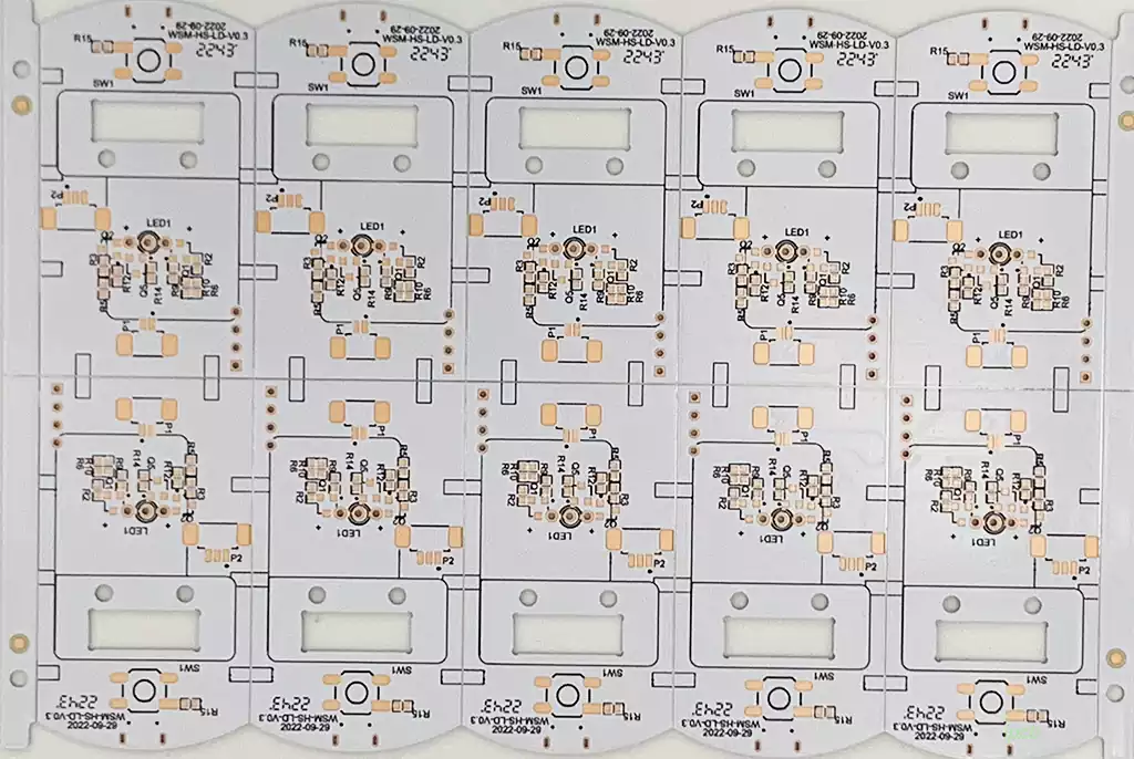
(6) short product development and market launch cycle, SiP in the functional analysis and division of the system, can make full use of the commercial production of chip resources, after a reasonable circuit interconnection structure and package design, easy to modify, production, and strive to achieve the best way and the lowest cost to the system’s design performance, no need to layout and wiring like SoC layout level, thus reducing the design, verification, debugging This reduces the complexity of design, verification, debugging and the time to realize mass production of the system, which can save more system design and production costs than SoCs, and the time to market can be reduced by at least 1/4;
SIP package types:
From the current industry SIP design type and structure distinction, SIP can be divided into three categories.
2D SIP
This type of package is in the same package substrate will be arranged one by one chip in a two-dimensional pattern packaged in a package body.
Stacked SIP
This type of package is a package in which two or more chips are physically stacked and integrated.
3D SIP
This type of package is based on the 2D package, the multiple Luo chip, package chip, multi-chip or even wafer for stacked interconnection, constituting a three-dimensional package, this structure is also known as stacked 3D package.
With the continuous development of SoC (system-on-chip) and SiP (system-in-package) technologies, PCB design is ushering in an unprecedented integration revolution. SoC has become an indispensable core component in modern electronic products with its advantages of efficient integration, low power consumption, high performance and low cost. SiP technology, on the other hand, integrates multiple chips and components into a single package through advanced packaging processes, further enhancing the integration and performance of the system.