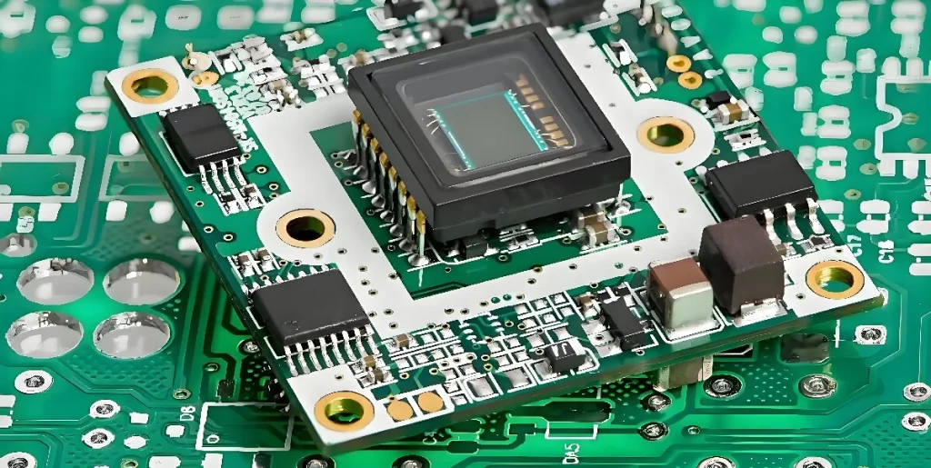
High-Density Interconnect (HDI) PCBs, with their finer line widths, smaller via diameters and higher routing density, have become indispensable core components in sectors such as smartphones, high-end telecommunications equipment and automotive electronics. However, compared to traditional PCBs, the manufacturing costs of HDI PCBs are significantly higher, presenting a practical challenge that many companies must address during the product design and mass production phases.
Factors Affecting HDI PCB Costs
Materials
Material costs form the cornerstone of HDI PCB costs, accounting for approximately 30%–45% of the total cost. The choice of materials directly determines the upper limit of HDI PCB performance and the lower limit of costs, and is one of the key factors influencing cost variations.
HDI PCBs demand far higher precision and stability from materials than standard PCBs, with price differences between materials potentially reaching several times the cost. Selecting materials appropriately is the first step in cost optimisation and the most easily achievable area for improvement.
As the core substrate of HDI PCBs, the substrate accounts for over 60% of total material costs and is the primary source of variation in material costs. FR-4 substrates, commonly used in standard consumer electronics, are relatively affordable, costing approximately 150–300 yuan per square metre.
In contrast, high-speed Low Dk/Df substrates and high-frequency PTFE substrates required for high-end telecommunications and automotive electronics can cost 800–3,000 yuan per square metre, or even more. This price disparity is directly reflected in the cost of the final product.
Furthermore, the thickness and number of layers of the substrate also influence costs. As the number of layers increases, substrate consumption grows exponentially, driving up costs; a 12-layer HDI substrate requires nearly three to four times the amount of material used in a 4-layer substrate.
Auxiliary materials such as copper foil, solder mask ink and surface treatment materials also have a direct impact on costs. The choice of copper foil thickness is directly proportional to cost; the cost difference between 1 oz and 2 oz copper foil can exceed 15%.
Furthermore, copper foil prices fluctuate in line with LME copper prices, indirectly affecting HDI PCB costs. Regarding solder mask ink, standard liquid photoresist solder mask is approximately 30% cheaper than dry film solder mask and is suitable for HDI products without ultra-fine lines.
Processing
Processing costs represent the core component of HDI PCB costs and are the key reason why HDI PCBs are more expensive than standard PCBs. The high-density and high-precision characteristics of HDI PCBs necessitate more complex manufacturing processes. With more sophisticated equipment and stricter quality control, every upgrade to a process results in a significant increase in costs.
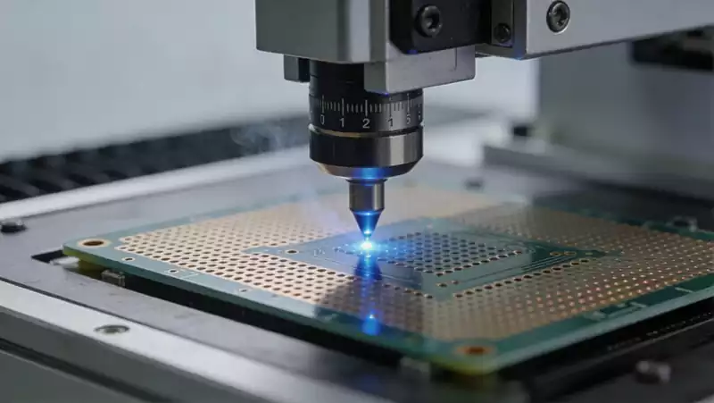
Laser drilling is a core process in HDI PCB manufacturing and represents the primary component of process costs. The microvia diameters in HDI PCBs typically range from 0.1 to 0.2 mm, or even smaller, necessitating the use of high-precision UV laser drilling machines.
Drilling costs are directly related to hole diameter and the number of holes—the smaller the diameter and the greater the number of holes, the longer the drilling time and the higher the cost.
Furthermore, the application of blind and buried via processes increases costs. This is because they require multiple laser drilling operations, interlayer alignment and lamination, resulting in a more complex process. This places higher demands on equipment precision and operator skill, and may consequently lead to an increase in scrap rates.
Design
Although design costs account for a relatively small proportion of the overall cost (approximately 5%–10%), they are a key hidden variable influencing cost overruns. Many companies, during the HDI PCB design phase, often over-emphasise performance redundancy whilst neglecting design manufacturability. This situation is particularly common in new product development, ultimately leading to issues such as complex processes, low yield rates and material wastage in subsequent production, thereby indirectly driving up overall costs.
Design complexity directly impacts costs; designs with line widths/spacing of less than 4 mil, excessive numbers of blind and buried vias, and irregular board shapes all increase processing difficulty and scrap rates. For example, widening the line width/spacing from 75/75μm to 100/100μm can reduce manufacturing difficulty and improve yield rates. Whilst this adjustment may seem minor, it can indirectly reduce cost losses by 5%–8%; conversely, an ill-conceived blind/buried via design may increase drilling difficulty and raise scrap rates by over 10%.
HDI PCB Cost Optimisation Strategies:
Design optimisation is the foundation of cost optimisation and represents the approach with the lowest investment and the most significant impact. During the design phase, one should avoid an excessive pursuit of performance redundancy; instead, simulation verification should be used to determine the minimum required number of layers and line width/spacing, thereby reducing the number of unnecessary blind and buried vias.
Optimise panel layout design and adopt panelisation to improve material utilisation; adhere to the manufacturer’s standard process parameters to avoid surcharges resulting from non-standard designs (non-standard designs typically incur a 20%–50% surcharge). For example, optimising a 10-layer HDI design to an 8-layer design can save 15%–25% in costs.
The cost of HDI PCBs is determined by three factors: materials, processes and design. Through sensible material selection, design simplification and process optimisation, effective cost control can be achieved without compromising product quality.
Material selection should adhere to a ‘balance of cost-effectiveness’, choosing appropriate materials based on the product’s application scenario and avoiding the ‘overuse of high-end materials’. For general consumer electronics, standard FR-4 substrates, OSP surface treatment and 1 oz copper foil can be selected to meet performance requirements whilst reducing material costs.
For high-end telecommunications and automotive electronics, high-speed and high-frequency materials should be selected as appropriate to ensure product reliability. Furthermore, a differentiated material configuration can be adopted to reduce material costs by 8–12% whilst maintaining performance.
Process adjustments can achieve cost optimisation through streamlining procedures and adopting alternative processes. Provided performance requirements are met, the number of blind and buried vias should be reduced, with through-holes used wherever possible; standardising via diameters and reducing the variety of laser drilling operations will lower processing complexity.
For line widths of 20 μm or greater, the sub-additive method can be used as an alternative to mSAP (modified semi-additive process) to reduce process costs. At the same time, hdi pcb production workflows can be optimised to improve equipment utilisation, reduce process waiting times, and lower unit process costs.
The cost of HDI PCBs is determined by three factors: materials, manufacturing processes and design. By selecting appropriate materials, simplifying the design and optimising the manufacturing process, effective cost control can be achieved without compromising product quality.