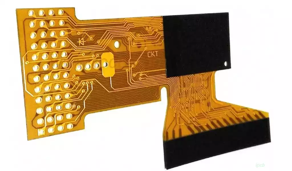
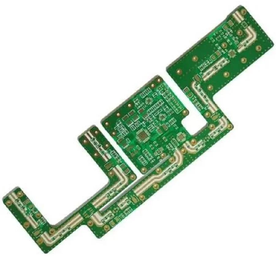
In the design and manufacture of circuit boards, pcb dimensions tolerance is a very critical issue that directly affects the effectiveness and performance of the circuit board.PCB board dimensional tolerances refer to the range of deviations allowed on the basis of set standard dimensions.Usually the dimensional tolerances of pcb plates are categorized into maximum and minimum dimensions, line widths, line spacing, and aperture diameters.
Dimensional Tolerances for Maximum and Minimum Dimensions
The dimensional tolerances of the maximum and minimum dimensions are a very important issue in the manufacture of printed circut boards. Manufacturing needs to ensure that the size of the board does not exceed the maximum value, but also can not be less than the minimum value, should be established in the product design phase of the corresponding standards. When the size of the pwb board exceeds the standard maximum or minimum value, will give the subsequent assembly work and the use of equipment has a great impact, and therefore need to be in the manufacturing of this before the close control.
Dimensional tolerances for line width and line spacing
In the manufacturing process, the printed wiring board on the line width and line spacing also need to be well controlled,the size of the deviation may be too large to make the line instability, short circuit or open circuit and other issues.Therefore,the width and line spacing of the lines should be reasonably designed according to the product design requirements when manufacturing the boards, and the dimensions should be effectively controlled to ensure the stability and connectivity of the lines.
Aperture size tolerance
In the electronic manufacturing process,the need for multiple aperture punching operations,at this time for the aperture size tolerances also need to be strictly controlled. If the aperture size does not meet the requirements, will have a great impact on the wire insertion,so that the conductive effect of the wire is affected, and in the use of the process of failure. Therefore, in the manufacture of printed circuit boards should pay attention to the control of aperture size, and in the manufacture of pre-design requirements based on the development of the corresponding aperture size tolerance standards.
Common size tolerance standards
PCB board size is one of the very important parameters in the manufacture of circuit boards, the size of the error will have a direct impact on the performance and productivity of the circuit board. Common board size standards include the following:
1.IPC-6012 standard: This is the International Institute of Electrical and Electronics Engineers developed printed wiring board manufacturing standards, including four product levels and five size categories, the most common of which are Class 2 products and Class 3 products. IPC-6012 standard requires that the circuit board dimensions should be within +/- 0.05mm, the tolerance should be controlled within +/- 0.1mm.
- GB/T 5237.4-2008 Standard: This is a standard issued by China’s National Organization for Standardization (NOS) for aluminum profiles, aluminum alloy profiles and aluminum profile products. For the size and tolerance requirements of circuit boards, the GB/T 5237.4-2008 standard is not as strict as the IPC-6012 standard.
- Other standards: In addition to IPC-6012 and GB/T 5237.4-2008, there are a number of international standards and regional standards, in terms of dimensions and tolerances are different.
Factors affecting the board thickness tolerance
Printed circuit board thickness tolerances are affected by a variety of factors, the most important of which are the following:
- The nature of the material: different boards on the board thickness control ability is different, therefore, in the selection of the board, you need to consider its ability to control the board thickness tolerance.
- Process control: plate thickness tolerance also depends on the control accuracy of the process such as pressure-sensitive film and cladding. Such as the choice of thin cladding process program, you can narrow the range of plate thickness tolerance.
- Manufacturing machinery and equipment: the accuracy and stability of manufacturing machinery and equipment will affect the actual manufacturing of pcb board thickness, so to ensure that the accuracy and stability of the equipment.
Adjust the circuit board thickness tolerance methods
- Material adjustment:
- Select a more stable thickness of the base material, you can reduce the board thickness tolerance.
- Selection of copper-clad foil with smaller thickness tolerance can adjust the thickness of the copper foil board to better control the board thickness tolerance. 2.
- Process adjustment:
- Selecting a finer cladding method can effectively reduce the board thickness tolerance range.
- The use of more delicate pressure-sensitive film process can improve the board thickness accuracy.
- Manufacturing equipment adjustment:
- Selection of high-precision manufacturing equipment can effectively improve the manufacturing accuracy, thereby reducing the board thickness tolerance range.
- Formulate a reasonable process to avoid human error, to ensure that the board thickness tolerance is more accurate.
The control of pcb dimensions tolerance is critical and has a direct impact on product performance. By precisely following standards, optimizing material selection, process control and upgrading equipment, we can effectively reduce tolerances and improve board quality.