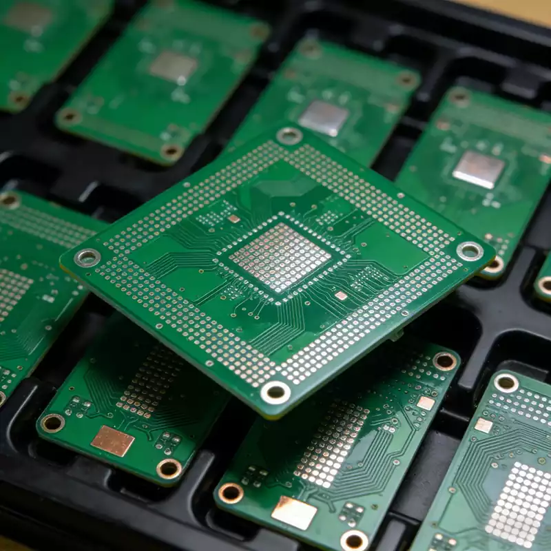
PCBs (printed circuit boards) serve as the “nerve centre” of electronic devices, bearing the core mission of signal transmission and electrical interconnection. Their performance directly determines the stability and reliability of electronic products, with the key to achieving this lying in a seemingly simple yet crucial process within PCB manufacturing: screen printing.
The core value of PCBs lies in establishing electrical interconnections between components, and screen printing is the pivotal process for forming the three critical functional layers: conductive traces, solder mask, and character layers. Unlike complex techniques such as photolithography and electroplating, screen printing occupies an irreplaceable position in PCB manufacturing through its straightforward logic of ‘stencil printing + paste curing,’ its role permeating the core stages of PCB production.
1.Conductive Circuit Printing
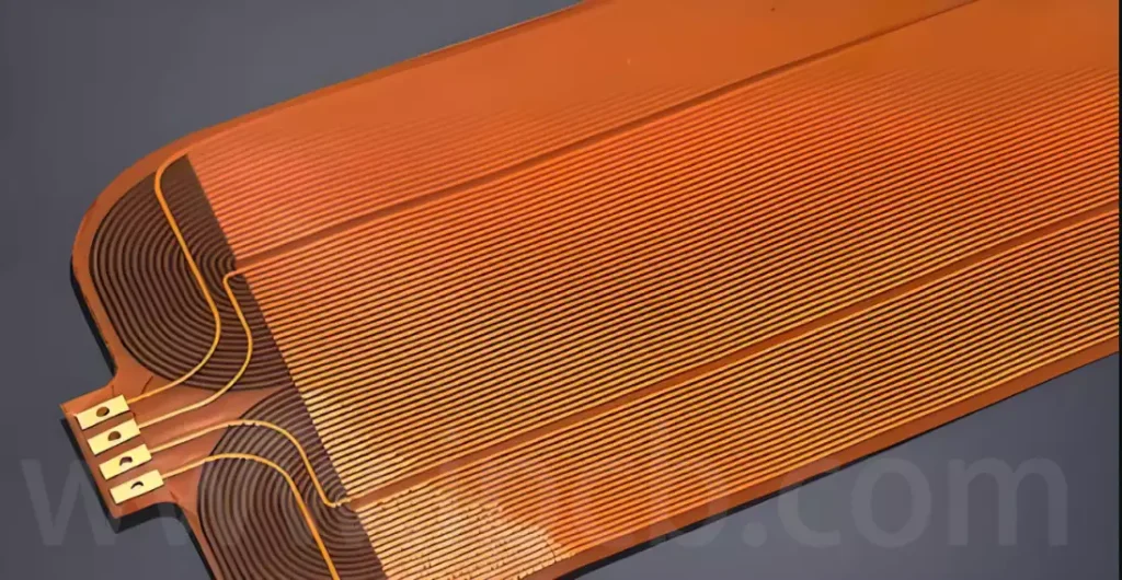
In the manufacture of specialised categories such as flexible PCBs and thick-film PCBs, screen printing serves as the direct method for forming conductive circuits. By transferring conductive pastes (silver paste, copper paste, carbon paste, etc.) onto the substrate surface through precision screen stencils, followed by high-temperature curing, it forms conductive circuits. This process replaces the etching techniques traditionally used in rigid PCBs. This process’s advantage lies in its avoidance of complex photolithography, development, and etching steps, making it particularly suited for forming circuits on flexible substrates. Flexible substrates possess high toughness but low corrosion resistance; etching processes readily cause substrate deformation, whereas screen printing’s non-etching nature perfectly circumvents this issue.
The printing precision of conductive circuits directly determines the PCB’s signal transmission capability. Taking flexible PCBs for 5G communication equipment as an example, trace widths and spacings must be controlled within 0.1–0.15mm. If screen printing registration deviations exceed 20μm, short circuits or open circuits may occur. Precise control of parameters such as mesh count, paste viscosity, and squeegee pressure becomes critical: Selecting a high-mesh screen of 300-400 mesh enhances edge definition. Controlling conductive paste viscosity between 10,000-15,000 cP prevents line widening due to paste spreading. Setting squeegee pressure to 0.3-0.5 MPa ensures uniform paste filling of mesh apertures without damaging the screen stencil.
2.Solder Mask Printing
The solder mask serves as an insulating protective layer covering the PCB surface, primarily preventing circuit oxidation, avoiding solder joint short circuits, and enhancing the PCB’s resistance to moisture, heat, and corrosion. Over 90% of solder mask formation relies on the screen printing process. The quality of solder mask printing directly determines the reliability and service life of the PCB.
A high-quality solder resist layer must meet three core requirements: uniform thickness, absence of bubbles, and absence of pinholes. Through screen printing, solder mask ink achieves uniform coverage across the PCB surface, with thickness precisely controlled between 20-30μm. It also enables precise blanking at pad locations according to design specifications. Key parameters in this process include: Selecting solder mask ink with excellent thixotropy prevents pad blockage caused by ink flow after printing; employing a stepwise temperature ramping mode during curing – ‘80°C pre-bake for 30 minutes + 150°C cure for 60 minutes’ – thoroughly expels solvents from the ink, preventing bubbles and pinholes post-curing.
Conversely, consequences of process failure include: insufficient solder mask thickness below 15μm leads to circuit oxidation in humid environments; inadequate ink curing causes cracking and delamination under high-temperature/humidity conditions; pad position deviations exceeding 10μm result in cold solder joints during component assembly. A consumer electronics manufacturer once experienced batch PCB production with locally insufficient solder mask thickness due to uneven squeegee pressure during printing. Consequently, the final products achieved only a 75% pass rate in salt spray testing, incurring substantial cost losses.
3.Character Layer Printing
The character layer comprises textual and symbolic markings on the PCB surface, serving to indicate component locations, polarity, model numbers, and other critical information. It forms an essential reference for PCB assembly, maintenance, and traceability. Character layer printing similarly relies on screen printing technology, with core requirements being ‘clear legibility, strong adhesion, and no flaking’.
Though seemingly straightforward, character printing demands rigorous attention to process details. Character inks must exhibit high adhesion and abrasion resistance. Printing requires precise alignment—character spacing from pads must be ≥0.2mm to prevent coverage and soldering interference. Simultaneously, character height and width must comply with industry standards: height ≥0.8mm and width ≥0.2mm to ensure visual clarity. For high-density HDI boards, character printing must also accommodate the layout of minute components. This necessitates the use of fine-mesh stencils and high-resolution film to prevent character overlap or blurring.
In large-scale PCB production, the process stability of screen printing directly impacts yield rates and manufacturing costs.
1.Screen Templates
Screen templates serve as the ‘mould’ for screen printing, with their manufacturing precision directly determining print quality. Core template parameters include mesh count, photosensitive emulsion thickness, and aperture accuracy, requiring precise selection based on PCB type and requirements.
Mesh Count: Higher mesh counts yield finer apertures and enhanced printing precision. Standard rigid PCBs typically require 200-300 mesh screens; HDI boards and flexible PCBs necessitate 350-450 mesh screens to ensure crisp formation of minute traces and characters.
Photoresist thickness: This determines the printed layer’s thickness. Solder mask printing requires 15-25μm photoresist, while character layer printing uses 5-10μm thin photoresist to prevent excessive thickness affecting assembly.
Opening precision: Stencil apertures must match PCB design drawings at a 1:1 scale. Opening edges should be smooth and burr-free, with alignment deviations controlled within ±10μm. High-precision stencils should be manufactured using laser cutting technology, replacing traditional chemical etching to enhance aperture accuracy and consistency.
2.Process Parameters
Regulating screen printing parameters is central to balancing precision and efficiency. During mass production, synergistic optimisation of three key parameters—squeegee pressure, squeegee speed, and printing gap—is crucial for improving yield rates.
Squeegee Pressure: Insufficient pressure prevents adequate paste filling of mesh apertures, resulting in insufficient layer thickness. Excessive pressure causes paste diffusion, leading to widened traces or blurred characters. For conventional PCB printing, squeegee pressure should be controlled between 0.2–0.6 MPa. Flexible PCB printing requires reduction to 0.1–0.3 MPa to prevent damage to the flexible substrate.
Squeegee speed: Excessive speed reduces paste filling time, increasing the risk of pinholes; insufficient speed prolongs paste residence in mesh apertures, causing ragged edges. During mass production, a squeegee speed of 50–100 mm/s balances efficiency and quality.
Printing gap: The distance between the screen template and PCB substrate. An appropriate gap ensures rapid separation after printing, preventing paste adhesion. Rigid PCB printing gaps should be 1-3mm, while flexible PCB gaps must be reduced to 0.5-1mm to prevent substrate deformation.
Advantages of Screen Printing
1.Cost-effectiveness
Screen printing equipment costs merely one-fifth to one-third of inkjet printing systems, with substantially lower consumables – stencils can be reused 5,000–10,000 times, significantly reducing per-unit PCB printing costs. For PCB factories producing tens of millions of units annually, screen printing can cut printing process costs by 30–50%. In contrast, while inkjet printing offers higher precision, its costly inks and complex equipment maintenance make it suitable only for small-batch, high-precision PCB production.
2.Mass Production Efficiency Advantage
Single-sided PCB printing cycles take merely 5-10 seconds via screen printing, far surpassing inkjet printing’s 30-60 seconds per board. It also enables continuous assembly line operations, aligning with large-scale mass production demands. In sectors with high PCB demand, such as automotive electronics and consumer electronics, screen printing’s efficiency is crucial for meeting delivery schedules. Furthermore, its flexible process adjustments allow switching between different printing patterns simply by changing the screen stencil, eliminating reprogramming and significantly reducing product changeover times.
3.Process Adaptability Advantages
Screen printing accommodates virtually all PCB types—rigid, flexible, HDI, thick-film, or high-frequency boards—by adjusting process parameters to achieve precise printing. For instance, in solder mask printing for high-frequency PCBs, low-dielectric-constant solder mask inks ensure uniform coverage via screen printing, safeguarding high-frequency signal transmission. In circuit printing for flexible PCBs, elastic squeegees and low-pressure parameters prevent substrate stretching and deformation. This extensive adaptability remains unmatched by other printing processes.
As the “unseen architect of circuitry” within PCB manufacturing, screen printing underpins the global PCB industry through its straightforward principles, precise control, and efficient mass production capabilities. From consumer electronics to automotive systems, from communication devices to aerospace applications, every reliably functioning PCB owes its precision to the screen printing process.