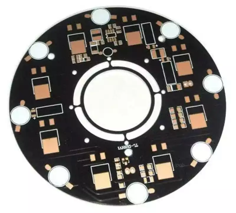
A 4 layer PCB, or four-layer printed circuit board, adds two internal copper layers to form a signal layer and a power layer compared to a double-layer PCB. As a result, the components on the PCB can be arranged more densely, resulting in smaller packages, higher levels of integration, and better immunity to interference. At the same time, the four-layer PCB can also realize signal transmission between multiple layers of boards through the lead-in of the internal copper layer, which further improves the transmission efficiency and reliability. Therefore, four-layer PCB has obvious advantages in high-speed transmission, high-density, anti-jamming and other aspects, is now widely used in computers, communications, automotive and other fields of a circuit board.
Four-layer PCB wiring rules
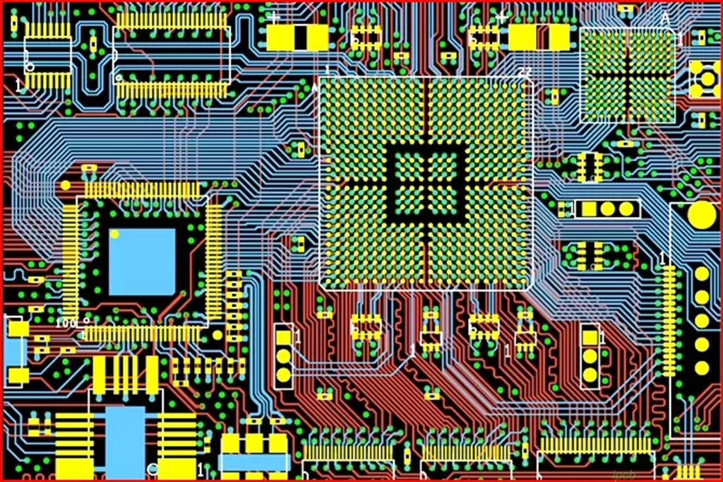
- Top layer design: This is the outermost layer of the PCB board, which is usually used for placing components and signal wiring. The wiring of the top layer design is like the main road of a city, which needs to be spacious and direct, avoiding too many bends and crossings to ensure the efficiency and accuracy of signal transmission.
- Ground Level Design: Immediately adjacent to the top layer design is the ground level, whose main role is to provide a stable reference ground plane for the entire PCB. The wiring of the ground layer should be as complete as possible,as a large net covering the entire level, to capture and stabilize the current and reduce noise interference.
- Power supply layer design: the power supply layer, located in the middle, is responsible for providing a stable power supply for the PCB.The wiring of the power supply layer should take into account the size and direction of the current, the reasonable layout of the power line and split the area,like a river system to transport energy to each place where it is needed.
- Bottom layer design: the bottom layer is usually used for auxiliary signal wiring and power wiring.The wiring of the bottom layer should try to avoid overlapping with the signal lines of the top layer design to reduce crosstalk and electromagnetic interference.
In the wiring process, the designer needs to be like a weaver who weaves fine patterns to precisely control the direction and spacing of the lines. Using modern PCB design software, designers can set up rules to automatically check the reasonableness of the wiring to ensure that every inch of the line meets the design specifications.
In addition, the wiring of a 4 layer PCB requires consideration of thermal management. Like finding shade on a summer’s day, designers need to ensure that heat can be effectively dispersed to avoid hot spots.This may involve designing thermal vias or thermal planes on the PCB to help transfer heat to other parts of the PCB or to external heat sinks.
Finally, the checking of the wiring after it is completed is indispensable.It’s like an artist’s review of a finished piece of work, needing to make sure that every stroke is just right. Designers use verification tools in their design software to check that the cabling meets electrical standards and that there are no potential signal integrity issues or manufacturing challenges.
Advantages of 4 layer boards over two-layer boards
The biggest advantage of four-layer boards over two-layer boards is circuit routing. The internal mezzanine of a four-layer board can be used for wiring, which allows for more complex circuit design and higher circuit density throughout the PCB. In addition, the wiring process is more flexible in a four-layer board, which helps the designer to realize more circuit functions. Therefore, four-layer boards can realize higher performance circuit functions through more complex designs.
The second advantage of four-layer boards over two-layer boards is the immunity to interference. Four-layer boards can better deal with electromagnetic interference in the design, through the ground layer and power layer design, can effectively reduce the electromagnetic interference in the circuit, improve the stability of the entire circuit.
The third advantage of the 4 layer board over the two-layer board is the signal transmission capability. The middle sandwich inside the four-layer board can be used to realize the separation and shielding of signals. This design can better prevent signal interference, thus making the signal transmission of the entire circuit more stable and reliable.
In addition to the significant advantages mentioned above, there are a number of other benefits associated with four-layer boards. For example, there is higher reliability and a relatively longer lifespan. In addition, due to the complexity of quad-layer boards, designers can make the wiring more compact through more layouts, thus reducing the size of the entire circuit board.
With its excellent performance and wide range of application prospects, the 4 layer PCB is driving the continuous development of the electronics industry. In the future, it will show its unique value in more fields.