In the surging tide of global hardware innovation and smart hardware iteration, from disruptive geek ideas in Silicon Valley garages to customized sensor terminals at the forefront of the Industrial Internet of Things, countless world-changing hardware innovations are transforming from abstract circuit diagrams into vibrant physical entities at an astonishing pace. On this challenging bridge connecting “theoretical concepts” and “mass production,” there exists a crucial, pivotal manufacturing hub—Small Batch PCB Assembly.
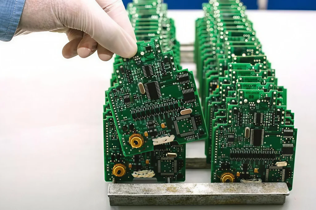
Unlike ultra-large-scale, highly automated production lines producing hundreds of thousands of units, Small Batch PCB Assembly focuses on customized, multi-variety, and rapidly iterating production needs ranging from tens to thousands of units. It is not a simple reduction of mass production, but an independent industrial science with extremely high demands on flexible manufacturing capabilities, engineering data preprocessing (DFM), changeover efficiency, and micro-metallurgical control. A deep dive into the underlying logic and manufacturing evolution of Small Batch PCB Assembly not only reveals the essence of modern agile hardware development but also showcases the ultimate art of micro-manufacturing engineering in balancing flexibility and high reliability.
Agile Development and Hardware Innovation
To understand the immense value of small-batch printed circuit board (PCB) assembly, we must first examine the harsh realities of modern electronic product development.
When hardware engineers complete the design of a completely new chip architecture and draw precise PCB schematics and layouts, they are not greeted with direct wealth and success, but rather with the dreaded “valley of death” in the hardware development field. During the design phase, no matter how advanced the computer-aided simulation (EDA), how the PCB performs under real electromagnetic environments, thermodynamic fields, and mechanical stresses remains highly unpredictable.
If a massive investment is made to establish a super-large automated production line with a capacity of millions of units, a tiny logical flaw in the circuit design or a pin definition conflict in a critical chip can instantly render the entire production line’s massive output of PCBs worthless industrial waste, causing enough economic losses to bankrupt a promising hardware startup.
Therefore, rigorous physical verification is essential before moving towards large-scale mass production. However, simply creating one or two hand-made prototypes for manual soldering in the lab is far from sufficient to realistically simulate the dynamic performance of automated mass production. Manual soldering cannot reproduce the high-precision solder paste rheology, guarantee perfect temperature profile control within the reflow oven, or expose coplanar defects or thermal stress hazards that only appear in large-scale continuous assembly.
It is against this backdrop that Small Batch PCB Assembly emerged. It precisely fills the gap between single-piece sample verification and mass production of millions of units. By providing high-precision machine assembly services on a scale of tens to thousands of units, it allows engineers to obtain the most realistic mass production quality data at extremely low overall cost and with extremely fast delivery cycles, thus safely navigating the “valley of death” in hardware innovation.
DFM Reverse Engineering and Supply Chain Restructuring Before Small Batch Production
The core advantage of mass production lies in “economies of scale.” Once a production line is calibrated, it can operate continuously for months or even years, with the initial engineering preparation costs infinitely diluted by the massive production volume. However, the fate of small-batch printed circuit board (PCB) assembly is “frequent line changes” and “varying product types.” This means that the engineering challenges of small-batch assembly begin even before the PCBs actually enter the machine shop.
Data Engineering and Precise DFM (Design for Manufacturing) Review
In small-batch production, time is of the essence. Engineers often expect to receive physical boards within days of order submission. This places extremely high demands on the initial data engineering conversion.
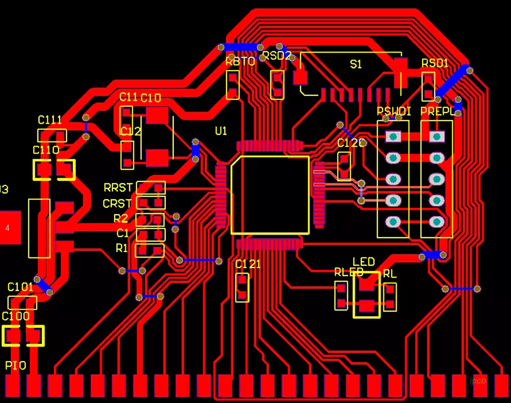
When customers upload Gerber production files, drilling files, and bills of materials (BOM) to a professional intelligent small-batch assembly plant, automation software and experienced process engineers immediately conduct an in-depth DFM review. Because small-batch customers often lack experience in large-scale mass production processes, designs often conceal fatal physical hazards: for example, pads designed too small causing “tombstoneing” during reflow soldering; solder mask bridges too narrow causing short circuits between adjacent pins; or surface mount pads directly connected to large copper areas causing severe localized heat sink effects and resulting in cold solder joints.
In small-batch printed circuit board (PCB) assembly, engineers must quickly correct and optimize manufacturing defects without altering the core circuit logic, generating perfect CNC machining data.
Dynamic Lifecycle Management and Global Sourcing of Bill of Materials (BOM)
If data engineering is the nerve center of small-batch production, then the Bill of Materials (BOM) is its body and blood. A major pain point for small-batch production lies in the extreme volatility and long-tail effect of the electronic component supply chain.
In mass production, factories can directly order batches of brand-new components from manufacturers, resulting in extremely low costs and high batch consistency. However, small-batch customers require a wide variety of components, potentially including various obscure chips, resistors and capacitors in different packages, and special sensors nearing the end of their lifecycle.
Small-batch PCB assembly service providers must establish a robust global intelligent sourcing network for electronic components and a digital warehousing system. The ability to procure dozens or even hundreds of distinct electronic components from thousands of compliant sources globally in the shortest possible time, while rigorously controlling production batches and MSL (Medium Static Electricity Level) ratings, is a key indicator of a small-batch assembly plant’s core competitiveness. The absence of any single component or its counterfeit status can bring the entire small-batch assembly process to a standstill.
Small-batch, highly adaptable solder paste printing and stencils
Once all components are ready and the bare circuit boards are prepared, the small-batch printed circuit board assembly enters its first physical stage in the manufacturing workshop—solder paste printing.
While mass production relies on expensive laser-cut stainless steel stencils and dedicated fully automated high-speed printing machines, stencil replacement frequency is extremely high in small-batch, multi-variety production scenarios. Achieving rapid and precise solder paste application is a complex discipline involving fluid mechanics and micro-geometry.
Stencil Micro-Aperture and Rheological Control
Solder paste is a complex non-Newtonian fluid composed of micron-sized metal alloy spheres and a high-viscosity thixotropic flux. In small-batch production, a single circuit board often contains both huge power chip pads and extremely small pads for micro-passive devices.
This necessitates highly sophisticated microscopic design in the stencil apertures. If the apertures for large pads are too large, excessive solder paste will be squeezed out during printing, causing component drift or short circuits during reflow soldering. Conversely, if the aperture ratio for small pads is misaligned, insufficient solder paste release will result in cold solder joints. Small-batch process engineers must customize the thinning, bridging, or geometric correction of each micro-aperture in the stencil based on the physical characteristics of the component packages to ensure that the solder paste is perfectly released from the stencil apertures and adheres to the copper pads at the moment the squeegee sweeps across at high speed.
Mold-Free Flexible Printing Adaptable to Multi-Product Changeover
In small-batch production lines striving for ultimate agility, advanced jet printing technology is shining brightly to save on the expensive costs and time associated with traditional dedicated stencil fabrication.
Jet printers completely break free from the constraints of physical stencils. Like high-end inkjet printers, they use piezoelectric ceramics to control tiny nozzles, directly “spraying” extremely small droplets of solder paste onto designated pad coordinates on the circuit board at extremely high frequencies. Regardless of the number of uniquely packaged components on the circuit board, the machine can complete the entire solder paste pattern changeover within one minute simply by modifying the CNC program in the computer. This mold-free flexible printing technology perfectly meets the ultimate desire of small-batch printed circuit board assembly for “multi-product, rapid changeover.”
Small-Batch SMT Placement and Multi-Product Feed Management
After solder paste printing, the circuit board immediately enters the high-speed placement stage of surface mount technology (SMT). This is also the most mechanically aesthetically pleasing industrial scene in small-batch printed circuit board assembly.
Dynamic Vision Calibration and Micrometer-Level Spatial Alignment
While modern small-batch placement machines don’t pursue the extreme speeds of hundreds of thousands of points per hour found in ultra-large-scale production lines, they place higher demands on their intelligent adaptability to “mixing various complex packages.”
When a circuit board is magnetically attached to the placement machine’s track, an onboard high-resolution industrial camera first rapidly scans the optical positioning points (mark points) on the board’s surface, establishing a dynamic two-dimensional physical coordinate system. Subsequently, the placement head picks up components from rapidly switching feeders. During its brief aerial journey to the circuit board, a bottom-mounted upward-looking vision system instantly images the component’s pins from multiple angles. Through complex image processing algorithms, it precisely calculates the component’s center offset and minute rotation angles, and a high-precision servo motor performs millisecond-level correction at the moment of descent.
Intelligent Feeder Management in Small-Batch Production
In small-batch assembly workshops, a single placement machine may need to handle dozens or even hundreds of different components simultaneously. Efficiently arranging and managing a wide variety of trays, strips, or bulk materials within limited machine space presents a significant engineering challenge that tests a factory’s on-site management capabilities.
Because small-batch orders often involve limited quantities of materials (e.g., a customer providing only the exact number of chips needed to assemble thirty wafers), pick-and-place machines must be extremely careful to avoid material loss due to the pull of the tape end when handling these valuable materials. Advanced small-batch production lines are equipped with intelligent quick-change feeders and barcode error-proofing systems. Operators simply scan the material label, and the system automatically verifies the BGM data, completely eliminating the catastrophic accident of manual material handling errors.
Reflow soldering and metallurgical bonding in small-batch mixed assembly
After hundreds or thousands of components of varying shapes are precisely placed on moist solder paste, the entire circuit board enters the core thermodynamic hub that determines its fate—the reflow oven.
In small-batch printed circuit board assembly, the reflow soldering process faces a unique physical challenge: the extreme non-uniformity of heat capacity distribution.
Temperature Profile Control to Address Differences in Heat Capacity
Small-batch circuit boards often integrate various functional experimental modules, their surfaces ranging from heavy, multi-layered copper power supply heat sinks and massive electromagnet transformers to ultra-miniature resistors and capacitors as small as grains of sand.
In different temperature zones of the reflow oven, these components of varying sizes and materials absorb heat at drastically different rates. If the oven temperature profile is improperly set, small-volume components may burn out due to excessively rapid heating or experience overheating and boiling of the solder paste, while large-volume components may suffer from cold solder joints because their slow heat absorption prevents some solder from reaching the eutectic melting point.
Small-batch process engineers must possess a strong foundation in thermodynamics. They need to meticulously craft customized oven temperature profiles for each unique small-batch product, optimizing the heating slope in the preheating zone and extending the holding and activation time to ensure that all solder joints on the entire board achieve near-synchronous temperature saturation and perfect melting when entering the peak reflow zone.
Instantaneous Growth of Microscopic Metallurgy and Intermetallic Compounds
Within the peak temperature range of reflow soldering, the fine alloy powder in the solder paste transforms into a liquid metal with extremely high surface tension. The liquid metal rapidly wets the copper pads and diffuses at the interface, growing a micron-sized intermetallic compound (IMC).
This extremely thin alloy layer forms a molecular-level bridge connecting components and the circuit board. In small-batch production, due to slight batch variations in surface treatment processes (such as immersion gold, plating, OSP, etc.) and component lead plating, the reflow soldering process must push metallurgical control to the extreme. Solder joints must not be too brittle and prone to detachment due to insufficient heat, nor should the IMC layer become excessively thickened and prone to brittle fracture due to excessively long high-temperature cycles.
Small-batch quality assurance and flexible testing engineering: While large-scale production has a large budget for customized large-scale testing fixtures and automated optical inspection lines, small-batch printed circuit board assembly requires a more flexible, efficient, and comprehensive quality assurance and testing system.
The Flexibility Advantages of Flying Probe Testing
In electrical performance verification, small-batch circuit boards typically forgo the costly and time-consuming traditional “bed-of-nails” testing fixtures. Instead, flying probe testing technology is employed.
Several extremely flexible, hair-thin test probes, driven by ultra-high-precision servo motors, move at astonishing speeds across both sides of the circuit board. Based on netlist data in a computer, they precisely contact every node, pad, and via on the board, instantaneously applying minute test currents and voltages to systematically check for open circuits, short circuits, and excessive resistance. Flying probe testing requires no custom-made physical hardware fixtures, perfectly matching the agile nature of small-batch production, enabling “on-demand modification and instant testing.”
Collaborative Screening with Machine Vision and Intelligent AOI/X-Ray
For assembly appearance and soldering quality inspection, small-batch production lines also incorporate advanced automated optical inspection (AOI) and X-Ray 3D non-destructive testing systems.
AOI (Automated Optical Inspection) can quickly capture the three-dimensional surface contours of solder joints using multi-angle color light sources, instantly identifying minute misalignments, insufficient solder, tombstone effects, or bridging short circuits. For the widely used BGA chips and QFN packages with solder joints on their chassis, X-ray penetration equipment can non-destructively “see through” the microscopic world beneath the chip, accurately detecting internal solder void rates. This flexible quality inspection network combining hardware and software ensures that every small-batch board delivered to customers possesses reliability comparable to mass-produced industrial-grade products.
Digital Twins and Intelligent Small-Batch Manufacturing
Looking to the future from the present perspective, small-batch printed circuit board assembly is undergoing a profound transformation driven by artificial intelligence, cloud computing, and the Internet of Things.
The traditional cumbersome model of “customers sending documents, factories providing manual quotations, and repeated telephone communication regarding processes” is being replaced by fully automated cloud-based intelligent quotation and manufacturing execution systems (MES). Engineers only need to upload design files in a browser, and the system will automatically complete DFM review, real-time component inventory matching, intelligent production scheduling, and accurate quotation within seconds.
Inside the workshop, digital twin technology is beginning to demonstrate its capabilities. Every small-batch production line, every pick-and-place machine, and every reflow oven is virtualized and mapped into a cloud-based digital space. Through deep learning from massive amounts of historical production data, artificial intelligence algorithms can automatically predict the most likely defects to occur during trial production of a new circuit board and proactively offer parameter optimization suggestions to process engineers. This intelligent small-batch PCB assembly model, which perfectly blends extreme flexibility with deep AI empowerment, is becoming an indispensable and powerful engine driving global technological innovation and hardware incubation at an unprecedented pace.
Conclusion
Small-batch PCB assembly is far more than just a simplified version of traditional electronics manufacturing; it is the most dynamic and precise art form within the modern agile software and hardware development ecosystem.
From digital preparation encompassing data engineering and intelligent sourcing, to flexible SMT production lines utilizing microfluidic jetting and dynamic visual correction; from thermodynamically balanced reflow soldering to flexible and efficient flying probe electrical verification, every step of small-batch assembly shines with the brilliance of human engineering wisdom on the micrometer and millisecond scale. It is precisely this efficient, reliable, and highly flexible manufacturing service that silently supports us behind the scenes, enabling countless geeks’ inspirations to quickly translate into world-changing technological products, continuously injecting an innovative future full of infinite possibilities.