The Physical Nature and Standard Evolution of FR4 pcb Thickness
In the field of printed circuit board (PCB) manufacturing, FR4 (Flame Retardant Rating 4) is not only a material but also a cornerstone of the electronics industry. When we discuss FR4 PCB thickness, we are actually discussing a core variable that affects the mechanical strength, electrical performance, heat dissipation efficiency, and package size of the final product.
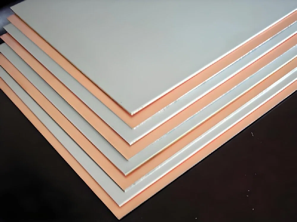
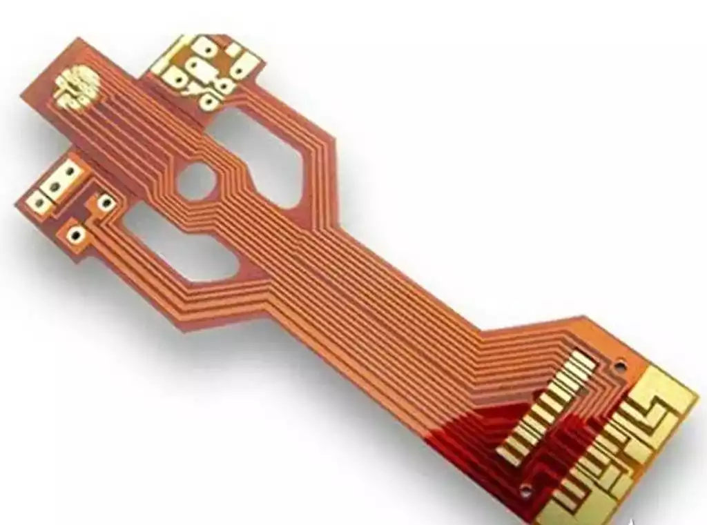
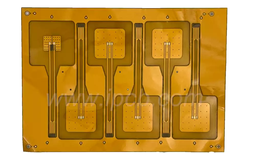
What is the “standard” for FR4 thickness? In the early days of the industry, 1.6mm (0.063 inches) was defined as the standard thickness. This figure did not originate from complex physical calculations but was a historical coincidence—early laminates were mainly used for slot-type connections, and the slot spacing of telecommunications equipment at the time just matched this specification. However, with the rapid development of microelectronics technology, a single 1.6mm could no longer meet diverse needs. Current thickness specifications typically range from 0.2mm to 3.2mm or even thicker. For multilayer boards (MLBs), the total thickness is the result of the core board, prepreg (PP), and outer copper foil layers stacked together.
The thickness of FR4 PCBs is primarily controlled by three key physical components:
- Fiberglass cloth type: Types such as 1080, 2116, and 7628, with different fabric densities determining the base thickness.
- Resin content: The degree of resin filling not only affects thickness but also directly relates to the dielectric constant (DK).
- Copper foil weight: Increasing copper thickness from 0.5 oz to 3 oz significantly alters the final measured thickness of the PCB.
The relationship between thickness and mechanical stress: In surface mount technology (SMT) assembly, board thickness directly determines the PCB’s resistance to warping. Thinner boards (e.g., 0.8 mm) are highly susceptible to deformation due to thermal expansion coefficient (CTE) mismatch when passing through a 260°C reflow oven. Therefore, in the pursuit of thinner and lighter smartphones and wearable devices, engineers must find a precise balance between thickness reduction and mechanical strength.
The Relationship Between Electrical Performance, Impedance Control, and Thickness
In high-speed digital circuit design, FR4 PCB thickness is not merely a physical dimension; it directly determines the characteristic impedance Z0 of the transmission line.
Mathematical Relationship Between Dielectric Thickness and Impedance
According to the microstrip impedance calculation formula, the characteristic impedance is directly proportional to the dielectric thickness h.
Simply put, when the signal line width is fixed, the thicker the dielectric layer (Core or Prepreg), the wider the electric field distribution, increasing inductance and decreasing capacitance, thus leading to increased impedance.
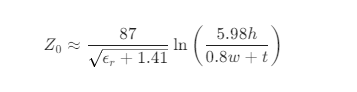
Where h represents the dielectric thickness, w is the conductor width, t is the copper thickness and the er refer Dielectric constant.
In modern multilayer board design, to achieve common 50Ω or 100Ω differential impedances, engineers must accurately calculate the thickness of each FR4 layer. If the thickness deviation during lamination exceeds 10%, it can lead to severe signal reflection and EMI (electromagnetic interference) problems.
Signal Loss and Dielectric Thickness
In high-frequency applications (such as 5G or radar equipment), thickness has a significant impact on signal attenuation. Thicker FR4 means longer via lengths, which introduces additional parasitic capacitance and inductance (via stub). At frequencies above 10 GHz, these subtle thickness differences can cause phase distortion.
Thickness Management in Multilayer Board Stackups
The final thickness of a multilayer board is “stacked.” This is not only a physical superposition but also a game of thermodynamic properties of the materials. The combination of a core board and a prepreg: The core board is a pre-cured FR4 sheet with copper plating on both sides, resulting in a relatively stable thickness. The prepreg (PP) undergoes rheological changes during lamination.
Adhesive Flow Control: If there is less residual copper foil, the final thickness after PP filling will be thinner than the nominal thickness.
Non-uniformity: In high-density interconnect (HDI) boards, non-uniform thickness distribution leads to decreased yield.
Lamination process tolerances challenge standard industrial tolerances, which are typically ±10%. This means that a board material nominally 1.6mm thick is considered acceptable if the actual measured thickness is between 1.44mm and 1.76mm. However, for precision aerospace electronics, requirements may be ±5% or even more stringent. This necessitates extremely high precision control over press pressure and temperature profiles during manufacturing.
The Trade-off Between Heat Dissipation Efficiency and Current Carrying Capacity
With the widespread adoption of power semiconductors (such as gallium nitride, GaN), the thermal conductivity of FR4 (typically only 0.25 W/m·K) has become a bottleneck.
Advantages of Thin Boards: Reducing the thickness of FR4 PCBs shortens the distance from the heat source to the heat dissipation surface (such as the bottom copper foil or metal casing), reducing thermal resistance.
Advantages of Thick Boards: While thick copper boards increase the overall thickness, they can carry hundreds of amperes of current, making them suitable for power distribution units in new energy vehicles.
Thickness Selection Guide for Different Application Scenarios
In practical engineering, choosing the right FR4 PCB thickness isn’t simply about being thicker for stability, nor is it about being thinner for advancement; rather, it’s about the art of “scenario adaptation.”
Consumer Electronics: The Challenge of Ultra-Thinness
In smartphones and smart wearable devices (such as the Apple Watch), PCB space is measured in micrometers.
Selection Habits: Typically, ultra-thin FR4 PCBs of 0.4mm, 0.6mm, or even 0.2mm are used.
Technical Challenges: At this thickness, the board is as flexible as paper. During SMT assembly, a “carrier” must be used to prevent the board from collapsing due to hot air or gravity in the reflow oven.
Industrial Control and Power Electronics: Durability First
Industrial PLCs and servo drives are often installed in environments with vibration and high temperatures.
Selection Habits: 1.6mm or 2.0mm are the mainstream.
Advantages: The thicker FR4 PCB provides excellent mechanical support, capable of supporting large electrolytic capacitors and heavy heatsinks, and is less prone to micro-cracks under long-term vibration.
Automotive Electronics: Rigid Requirements for High Reliability
Automotive-grade PCBs (AEC-Q100 standard) have extremely stringent thickness tolerance requirements.
Multilayer Trend: With the increasing computing power of autonomous driving, 8-layer and 12-layer boards are becoming the norm. To accommodate more layers while maintaining the total thickness (typically 1.2mm or 1.6mm), the dielectric layers must be thinned, placing extremely high demands on the dielectric breakdown voltage of FR4.
Manufacturing Limits and Cost Balance
Why is 1.6mm cheaper, while 0.2mm or 3.2mm is expensive? The underlying logic is manufacturing efficiency.
The “Yield Tax” of Ultra-Thin PCBs
When FR4 PCB thickness is less than 0.4mm:
Shrinkage Control: Dimensional shrinkage of inner layers during etching and lamination is extremely difficult to predict.
Open Circuit Risk: Mechanical drilling can easily tear the ultra-thin substrate.
Automation Limitations: Standard horizontal production line conveyor rollers may get caught in the thin board.
The “Process Tax” of Ultra-Thick PCBs
When board thickness exceeds 2.4mm:
Drilling Challenges: Drill bits are prone to deflection in thick boards, and chip removal is difficult, leading to increased hole wall roughness.
Electroplating Capability: An excessively high aspect ratio makes it difficult for plating solution to penetrate to the center of the hole, resulting in uneven copper thickness on the hole walls.
Cost Curve
1.0mm – 1.6mm is at the bottom of the cost curve. Once outside this range, whether going down (thin) or up (thick), for every additional 0.2mm of special requirements, the cost can increase by 15%-30%.
Summary: Towards a Future of Precision Manufacturing
Choosing FR4 PCB thickness is a multi-dimensional trade-off. From initial physical support to mid-term impedance control, and now to heat dissipation and high-frequency loss management, every micrometer change in thickness affects circuit stability.
For buyers and engineers, understanding the manufacturing tolerances, dielectric losses, and cost premiums behind thickness is key to achieving commercial success. In the future, with the widespread adoption of HDI and embedded component technologies, our control over thickness will enter an era of “atomic-level” precision.