“A Rock-Solid ‘Third Hand’: The Mechanical Essence of PCB Board Holders in Manual Soldering”
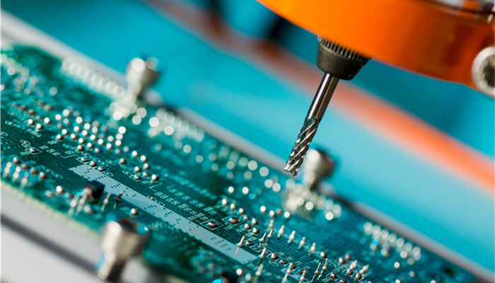
In the R&D, prototyping, and after-sales repair stages of electronic products, although automated surface mount technology (SMT) lines can complete chip soldering at millisecond speeds, manual soldering and testing remain indispensable critical steps. For example, manually soldering bulky connectors onto freshly soldered bare boards, debugging sensitive RF signals, or using oscilloscope probes to capture fleeting waveform defects.
In these highly focused micro-operations, even the slightest hand tremor can cause the soldering iron tip to overheat and damage nearby microcapacitors, or cause test leads to slip, directly resulting in a short circuit. At this point, a high-quality PCB circuit board holder… This has become an indispensable “third hand” on an engineer’s desk. It’s not just a simple physical clamp, but a physical and mechanical framework ensuring soldering accuracy and operational safety.
The Spatial Game of Counterweight and Center of Gravity: Preventing “Tilting Over” Tragedy Many novice hardware engineers, when purchasing workbench tools, often opt for extremely thin clamps made of thin iron sheets or even plastic, prioritizing cost. However, in actual use, such low-end clamps can be a major disaster.
When debugging a multi-layered motherboard covered in chips and possessing considerable weight on a desktop, if the clamp’s counterweight is insufficient, its center of gravity will become extremely high. When you forcefully press down with a spring-loaded test probe or solder pins with heavy multi-strand power cables, the applied mechanical torque will instantly disrupt the balance, causing the clamp, along with the entire expensive prototype, to collapse on the workbench, resulting in a “tilting over.” This can lead to anything from broken wires to a hot soldering iron tip striking the operator’s arm, causing a serious safety accident.
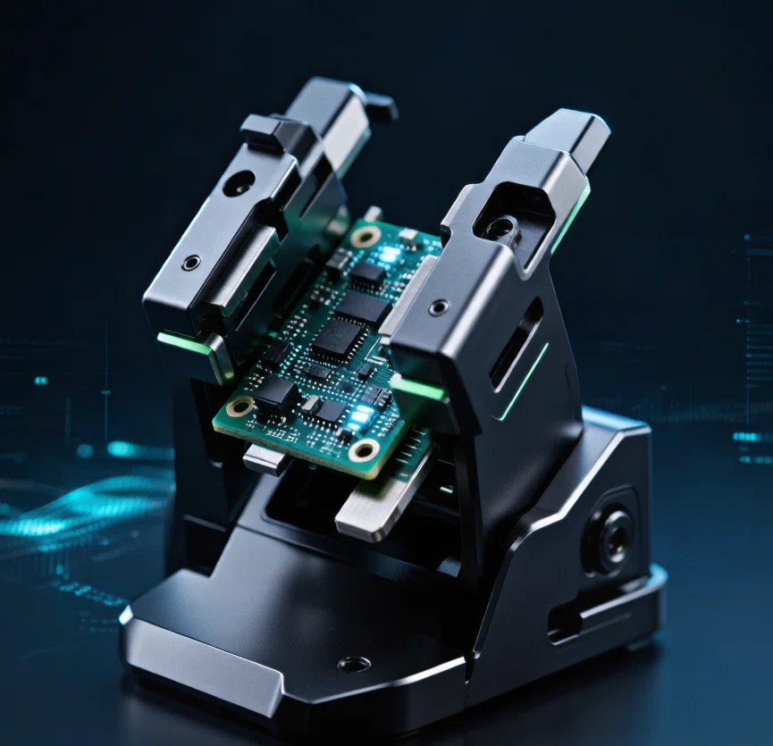
Therefore, top-tier industrial-grade PCB circuits… In terms of structural design, the primary challenge for board holders is “chassis mechanics.” Their bases are typically made of extremely heavy, solid cast iron, solid steel plates, or thickened anodized aluminum alloy.
By concentrating over 70% of the weight on the bottom layer closest to the desktop, the overall center of gravity is significantly lowered. Even when engineers exert force by inserting, prying, or using a hot air gun for 350-degree Celsius soldering, the base remains firmly anchored to the workbench like a suction cup, achieving true “rock-solid stability.”
The Material Aesthetics of the Clamping Mechanism: Protecting Delicate Bare Board Edges
Besides a stable base, the material selection and mechanical structure of the “gripping claw” (the part of the clamp that directly contacts the circuit board) are equally crucial.
The edges of circuit boards are actually very fragile at a microscopic level. Especially with high-precision HDI boards, to achieve the ultimate in space optimization, engineers often run extremely fine signal traces close to the V-CUT edge of the circuit board. (The wire or stamp hole edge) extends all the way.
If the grippers use rough, purely hard metal screws to directly tighten onto the circuit board, the huge local compressive stress from the hard metal contact will instantly shatter the solder mask layer at the edge of the circuit board, and may even directly sever the hidden microscopic copper traces inside, causing an internal open circuit before the board is even soldered.
High-quality circuit board support grippers will inevitably adopt a “rigid-flexible” design. Its core framework is a high-strength guide rail, but the V-shaped contact surface directly with the circuit board… Inside the groove, a layer of special silicone rubber or Teflon gasket, possessing elasticity, high-temperature resistance, and chemical corrosion resistance, is perfectly embedded.
When the grippers close, the elastic gasket gently wraps around the edge of the circuit board, evenly distributing the concentrated mechanical shearing force across the entire edge. This provides excellent friction, ensuring the circuit board remains completely stable during 360-degree rotation, while perfectly protecting the ink and edge traces of the bare board from any physical damage.
360-degree multi-dimensional rotation and thermal management: the secret to efficient soldering.
Having solved the basic physical clamping and… After safety protection is implemented, the efficiency of manual soldering and repair depends entirely on the “degrees of freedom” of the support in three-dimensional space and its thermal performance under high temperatures.
Freedom of Three-Dimensional Joints: Say Goodbye to Awkward Soldering Postures
In manual soldering, the most taboo thing is for engineers to twist their wrists into extremely awkward positions to get close to the solder pads in order to accommodate the fixed circuit board. Maintaining this unnatural posture for a long time not only leads to rapid fatigue of the hand muscles, resulting in uncontrollable micro-tremors, but also causes cold solder joints because the view is blocked by the soldering iron tip.
Advanced PCB circuit board holders typically employ a ball joint or a dual-axis 360-degree independent rotation mechanical topology.
By releasing a central quick-lock knob, engineers can smoothly adjust the circuit board to any perfect angle with one hand.
For front-side surface mounting: Laying the board flat provides an excellent vertical viewing angle;
For soldering pins on the back: A gentle flick allows the board to flip 180 degrees, directly exposing the back side without needing to remove the board from the grippers for reinstallation.
This smooth spatial transformation allows the soldering iron tip to always elegantly contact the pads at the most ergonomic 45-degree angle, thus significantly improving the efficiency and aesthetics of manual soldering.
“Heat Stealers” and Localized Heat Management During Soldering
When manually soldering power boards or multilayer boards with large copper areas, engineers often complain: “I’ve set my soldering iron to 400 degrees, why isn’t the solder melting on the pads?” “It turns into a sticky mess the moment it touches the surface?”
Analyzing this process bottleneck reveals a clear problem: besides the rapid heat dissipation of the large copper foil itself, low-end metal clamps are also a major “heat thief.”
If your circuit board clamp uses large, uninsulated, pure metal jaws, when your soldering iron tip heats the pads, the heat flows continuously from the copper foil of the circuit board to the tightly clamped metal jaws. The massive size of the jaws is equivalent to hanging a horribly powerful heatsink on the edge of the board, frantically drawing energy away from the soldering iron, preventing the local temperature of the pads from rising and causing soldering failure.
To eliminate this process defect, high-end clamps employ extremely stringent thermal resistance design. The V-shaped… The soldering slot not only uses insulating materials with low thermal conductivity, but also typically features an extremely thin “skeleton structure” between the grippers and support rods to reduce the physical contact area. Through this microscopic thermal bridging design, heat is firmly trapped inside the circuit board, preventing the support from escaping precious heat and ensuring that the solder melts perfectly and smoothly the moment the soldering iron touches the pad, forming a beautiful, rounded solder joint.
Microscopic Hunting of Electrostatic Discharge (ESD): The Neglected Killer
Having completed the optimization of structural mechanics and thermals, we now enter a crucial area of manual work that is invisible and intangible, yet capable of instantly turning high-performance chips worth tens of thousands of yuan into scrap metal—electrostatic discharge (ESD).
The Paradox of “Electrostatic Accumulation” in Insulating Materials Many ordinary customers, unfamiliar with electronic assembly standards, often buy cheap circuit board brackets assembled from plastic or acrylic to save money or for aesthetic reasons. They believe that plastic is non-conductive and safe to place on a desk.
However, this is an extremely ignorant and basic mistake in the professional field of electronics manufacturing. Plastic is an absolute electrostatic insulator, meaning that once a charge is generated on its surface (e.g., through air friction or clothing friction), it cannot flow across the surface but instead accumulates locally like a “charge abyss.” Over time, the electrostatic voltage on the surface of the plastic bracket can easily build up to thousands or even tens of thousands of volts.
When engineers assemble a delicate circuit board with very large-scale integrated circuits (such as high-end…)… When bare PCBs (MCUs, FPGAs) are clamped onto this plastic bracket, the exposed pins of the chip, upon approaching these high-voltage electrostatic fields, will suffer instantaneous electrostatic discharge (ESD) due to the silicon dioxide insulating gate, which is only tens of nanometers thick inside the chip.
This discharge is microscopic, without any sparks or sound, but the microscopic circuitry inside the chip melts and breaks within a microsecond. The product may function perfectly during factory testing, but after a few days of use with the end customer, it may suddenly and inexplicably crash and become unusable. This is the “latent damage” that everyone in the industry fears.
How are truly ESD-compliant anti-static brackets made?
To completely eliminate ESD damage during manual soldering and debugging, professional PCB circuit board holders must undergo thorough “static dissipation” in materials engineering. The device undergoes a “Dissipative” modification.
Its surface is absolutely free of any ordinary plastic or acrylic. All non-metallic components must be forcibly mixed with a specific proportion of nano-scale highly conductive carbon fiber or antistatic additives during the material melting stage. This tightly limits the surface resistivity of the material to between 10⁶ and 10⁹ ohms.
This resistivity is remarkably subtle: it is neither a perfectly conductive material (preventing metal-to-metal short circuits during live circuit board testing) nor a perfectly insulating material. It allows the generated static charge to slowly and safely “flow and diffuse” across the surface.
Furthermore, a dedicated grounding jack is standardly installed at the edge of the base of the stand. This is achieved through a wire with a 1… The megaohm safety resistor’s anti-static grounding wire connects directly to the dedicated grounding grid in the laboratory or factory. This ensures that all microscopic static charges, whether generated in dry winter air or from friction between workers’ clothing, are gently and safely channeled into the ground via the anti-static grippers and conductive frame, ultimately flowing along the grounding wire. Static electricity is nipped in the bud, providing delicate chips with perfect electromagnetic protection.
From Laboratory to High-Efficiency Small-Batch Production Lines: The Supply Chain Landscape of Multifunctional Brackets
Having thoroughly explained the core details of a top-tier circuit board bracket in terms of mechanics, thermals, and anti-static properties, let’s examine its commercial role in the entire electronics industry supply chain and actual business operations. It’s not limited to single-chip debugging in R&D labs; it’s also crucial for many high-value-added, small-batch, multi-variety (Low-Volume) production lines. The secret weapon for improving labor efficiency in high-mix manufacturing companies.
The “modular patch panel” on manual assembly lines. In aerospace, medical device, and high-end smart grid instruments, order volumes are typically small, but the quality requirements for each solder joint are almost obsessively high, making fully automated wave soldering impossible. On these small-batch assembly lines, workers need to line up and manually touch up solder joints.
If workers were to solder boards flat on a table, it would not only be slow, but also prone to missed solder joints due to eye strain.
Modern factories equip each workstation with a standard modular circuit. Board supports. These supports typically feature an adjustable parallel double-rail system on both sides. One rail is fixed, while the other slides freely via a quick-release handle.
When a complete board (panel) is delivered after completing the previous process, the worker only needs to use one hand to clamp it, and the board perfectly embeds into the slots of the two rails. No screws need to be turned; the internal spring tension achieves a one-second locking. Patch placement, flipping, soldering, one-second release, and flow to the next process. Through this standardization and assembly-line transformation of mechanical movements, the uptime per person (UPH) of manual welding stations can be easily improved. Over 40% savings directly reduce labor costs for businesses.
Ultimate Procurement Guide: How to Choose the Perfect Fixture for Your Engineering Team
Reject Pure Plastic and Spring Clamps: Prioritize solid metal bases weighing at least 1.5 kg to ensure high-density multilayer boards remain stable under load.
Require ESD Certification: Clearly require the bracket’s grippers and surface coating to have anti-static dissipation capabilities, with impedance meeting international anti-static standards (EOS/ESD S20.20) to protect core FPGA/BGA chips.
Emphasize Axial Locking Durability: Inspect the locking mechanism at the joints. High-end brackets typically use gear-operated locking or high-hardness alloy ball valves, capable of withstanding tens of thousands of repeated tightening without stripping, preventing “joint loosening” and rickets after long-term use.