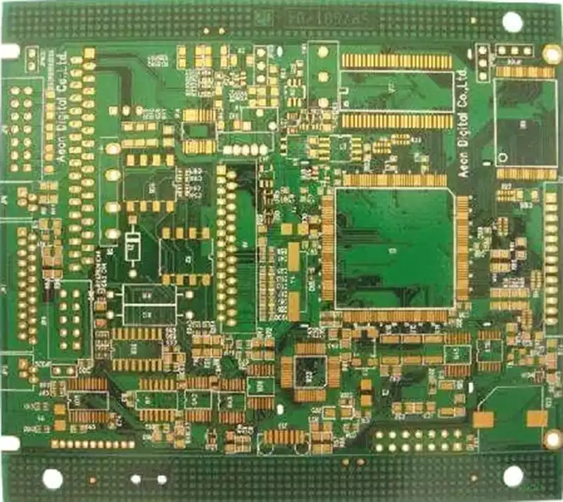
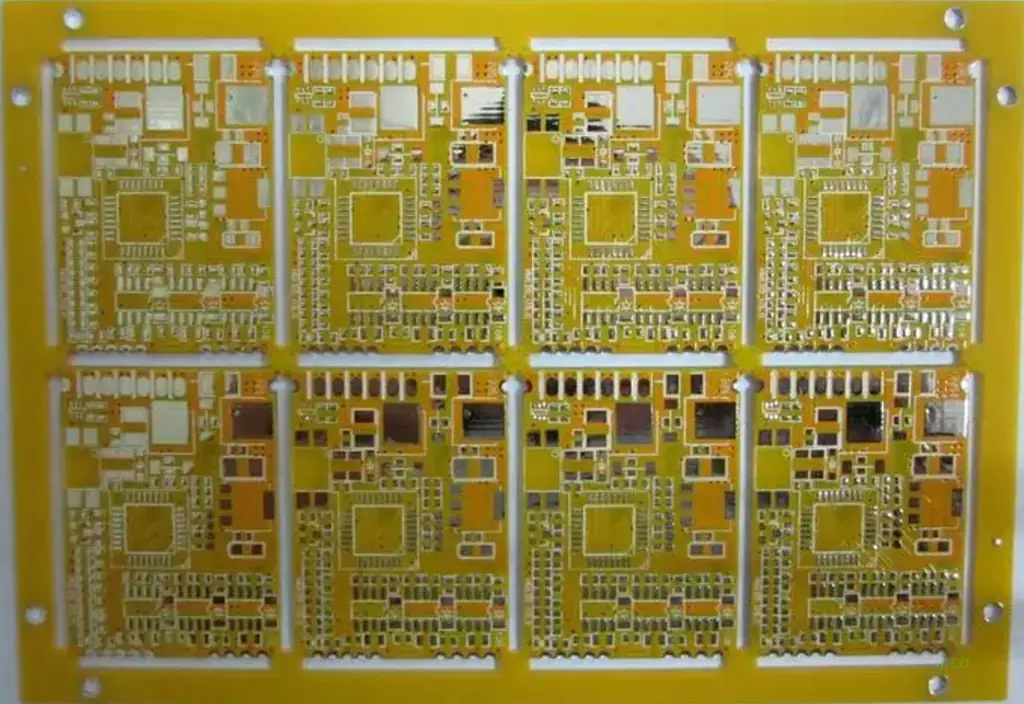
Conductive via holes, also known as through holes, pcb via must be filled to meet customer requirements. After extensive testing, the traditional aluminium plate filling process has been replaced with a white mesh to complete the solder mask and filling of the PCB surface. This ensures stable production and reliable quality.
Via holes serve to connect and conduct electrical signals between circuits. The development of the electronics industry has also driven the advancement of PCBs, placing higher demands on PCB manufacturing processes and surface mount technology. The via hole filling process has emerged to meet the following requirements:
(1) Copper is sufficient inside the via hole; solder mask may or may not be filled;
(2) The via hole must contain tin-lead with a certain thickness requirement (4 microns), and no solder mask ink should enter the hole to prevent tin balls from forming inside;
(3) Via holes must be filled with solder mask to prevent light penetration, and there must be no solder rings, solder balls, or unevenness.
As electronic products continue to evolve towards ‘lighter, thinner, shorter, and smaller’ designs, PCBs are also moving towards higher density and greater complexity. This has led to an increase in PCBs using SMT and BGA technologies. Customers often require via hole filling during component placement, primarily for the following five purposes:
(1) To prevent solder from penetrating through the via holes to the component side during wave soldering, causing short circuits; especially when placing vias on BGA pads, via filling must be performed first, followed by gold plating, to facilitate BGA soldering.
(2) To prevent flux residues from remaining inside the via holes;
(3) After surface mounting and component assembly are completed, the PCB must be subjected to vacuum suction to create negative pressure during testing;
(4) Prevent surface solder from flowing into the vias, causing cold solder joints and affecting assembly;
(5) Prevent solder balls from being ejected during wave soldering, causing short circuits.
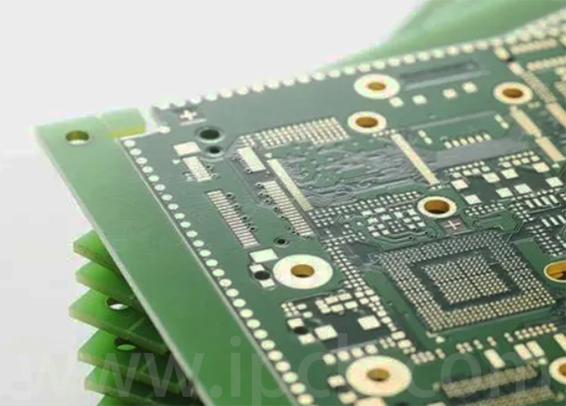
Why is PCB via filled?
- Electrical isolation and prevention of short circuits
Blocking the vias on a PCB achieves electrical isolation, preventing unintended short circuits between conductors or electrical components on different layers. In certain special applications, maintaining electrical isolation between different layers of the PCB is necessary to enhance circuit stability and reliability. Blocking the vias prevents any current or signals from propagating between layers, thereby avoiding incorrect circuit connections and interference. - Improving signal integrity
Filling via holes on a PCB can also improve signal integrity. When signal lines pass through via holes, signals may be affected by loss, interference, and crosstalk. Filling via holes reduces these adverse effects, improving signal transmission quality and stability. Especially for high-speed and high-frequency signal transmission, maintaining signal integrity is critical for the proper and reliable operation of the circuit. - Improve signal integrity
In high-frequency and high-speed digital electronic devices, such as computers, mobile phones, and communication equipment, signal integrity is critical to circuit performance and reliability. For these applications, a series of measures are typically taken during PCB design and manufacturing to improve signal integrity, one of which is to fill vias. This is because vias may cause incomplete signal loops and interference, thereby affecting signal transmission and reception. - Improving Circuit Performance
By plugging the vias on PCB boards, circuit performance can be further enhanced. Vias may cause uneven material distribution on the circuit board, leading to unstable mechanical properties. By plugging the vias, material distribution unevenness can be reduced, thereby improving the mechanical strength and stability of the circuit board. This is particularly important for applications with high requirements for circuit board quality and reliability, such as aerospace, military, and medical equipment. - Reducing Manufacturing Costs
Although filling vias on PCB boards requires additional steps and processes, it can reduce manufacturing costs in certain situations. By filling vias, impurities and residual substances during electroplating and processing can be reduced, thereby improving manufacturing efficiency and quality. Additionally, filling vias can reduce the amount of electroplating solution used and waste disposal costs, thereby lowering production costs.
PCB via plugging is a critical process in modern PCB manufacturing. It not only effectively prevents soldering defects and improves signal integrity, but also enhances the mechanical performance of circuit boards and helps optimise production costs. These functions collectively ensure the high performance and reliability of electronic products in line with the trend towards ‘light, thin, short, small’ and high density.
