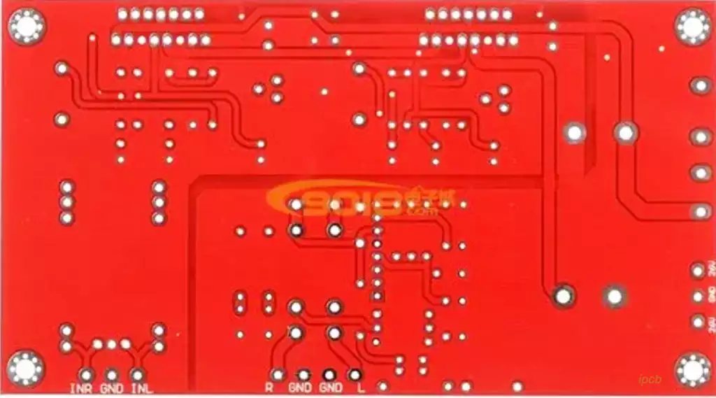
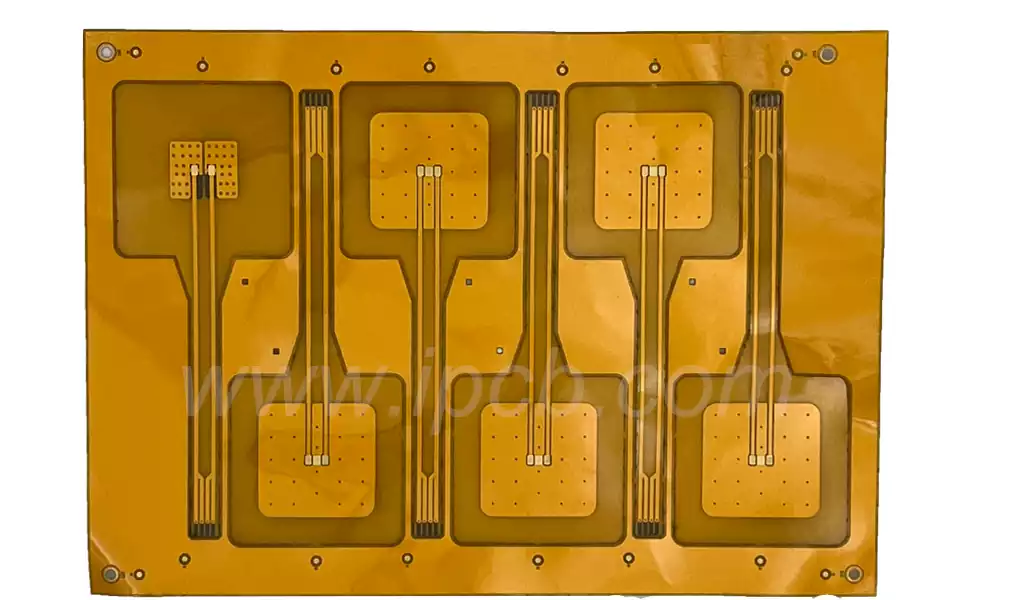
Flying probe test, as a kind of electronic circuit testing technology, is mainly used in the testing process of PCB (Printed Circuit Board), which is an indispensable means of non-contact testing. The technology utilizes a probe carried by a precision robotic arm to verify the connectivity of the circuit by approaching the test point without touching the surface of the PCB. With its high speed, high accuracy and no need to preset test points, flying probe test shows unique advantages in the inspection of high-density and complex PCB boards.
The difference between flying probe test and test rack is mainly reflected in the test method, cost and applicable scenarios. Flying probe test adopts 4 to 8 probes for high-voltage insulation and low-resistance conductivity test, without the need to make special test fixtures, just load the PCB board into the test machine and run the program to complete the test. This flexible and convenient testing method saves testing costs and time, and is especially suitable for small batch production. In contrast, the test frame is designed for mass production of PCB boards through the test fixture, although the production cost is higher, but the test efficiency is high, and return orders without additional charges. In terms of testing purpose, flying probe test is more suitable for small volume production and sample test, while test rack is more suitable for mass production scenarios.
The purpose of flying probe test mainly includes defect identification, performance verification, production optimization and quality assurance. It can quickly and accurately identify and locate defects in the manufacturing process, such as short circuits, open circuits, etc.; verify the electrical performance of the PCB to ensure that it meets the design requirements; optimize the production process through test feedback to improve the overall efficiency; and provide strict quality control for each PCB to ensure that it meets the industry standards and customer expectations.
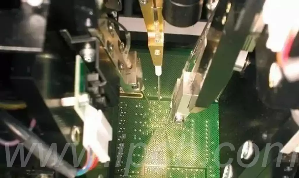
The working principle of flying probe test is based on the synergy of probes and cameras. Test probes are connected to drivers and sensors via a multiplexing system to test components on the PCB. During the test, cameras are used to assist in locating missing components and to check the shape and orientation of the components. With improved probe positioning accuracy and repeatability, flying probe testers are able to precisely probe components on PCBs and solve a large number of existing problems such as long test development cycles, uneconomical testing for small production runs, and slow testing of prototype samples.
The advantages of flying probe testing are its flexibility, high efficiency, cost savings, high accuracy, timely feedback and improved quality. It eliminates the need for specialized fixtures and is suitable for a wide range of PCBs of different designs, especially for low-volume or customized products; the test process is fast and parallel, significantly reducing overall test time; it eliminates the high cost of making fixtures and reduces initial investment and production costs; it efficiently detects problems using precision probes and advanced algorithms; it instantly detects defects during production, allowing manufacturers to make quick adjustments and repairs; and it ensures that each PCB is tested to the highest quality through Rigorous electrical testing ensures the quality of each PCB and enhances the reliability of the final product. In addition, the Flying Probe Test System is capable of performing In-Circuit Test (ICT) and Functional Test (FCT), further enhancing its application value.
