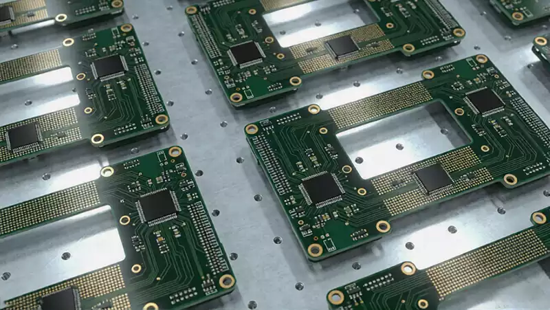
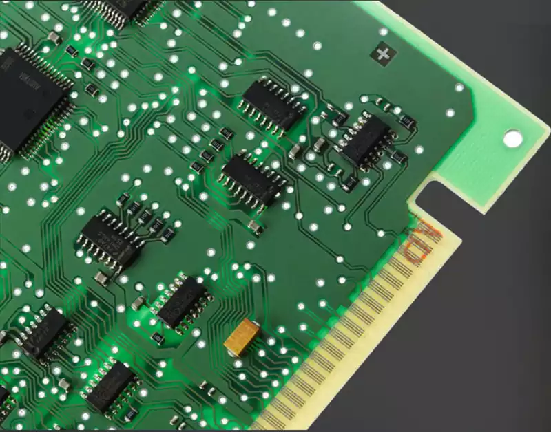
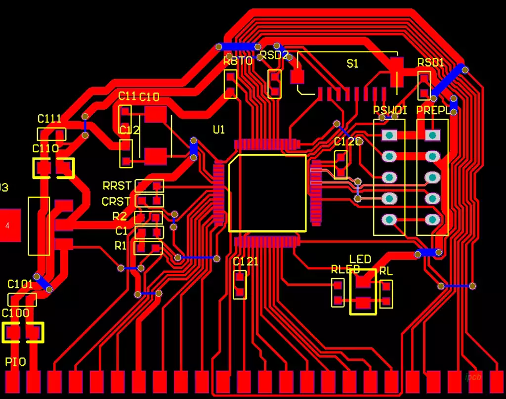
In the grand narrative of modern electronics industry, printed circuit boards (PCBs) are subjected to extremely demanding physical and electrical expectations. They must maintain absolute physical stability and electrical insulation under extreme temperature fluctuations, high-frequency electromagnetic interference, and high-density current surges. However, when these physical boundaries are broken, the laws of thermodynamics take over in the most destructive way. In the intersection of electronic engineering and environmental science, “burning circuit boards” not only represent a catastrophic hardware failure mode but also point to one of the most burdensome and controversial physicochemical transformation processes in the global e-waste disposal industry.
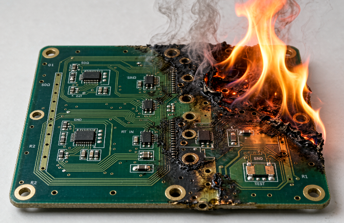
This is far more than a simple “fire” or “smoke.” From the microscopic breaking of polymer molecular chains and the quenching of flame retardant free radicals, to the macroscopic thermal runaway, carbonization, and conductive chain reactions, and finally to the dioxin ecological disaster caused by the open burning of e-waste, the combustion of printed circuit boards is a complex engineering physics problem spanning materials science, thermodynamics, electromagnetics, and environmental chemistry.
Thermodynamic Boundaries and Microscopic Flame-Retardant Chemistry of Polymer Substrates
To understand why printed circuit boards (PCBs) burn and what microscopic reactions occur during combustion, we must first dissect the physical and chemical properties of their core base materials.
The Physical Symbiosis of Epoxy Resin and Glass Fiber Most modern PCBs use composite material substrates, the most classic example being the well-known flame-retardant glass fiber epoxy resin copper-clad laminate. This material exhibits high anisotropy in its physical structure. Its skeleton is an insulating mesh woven from extremely fine glass fiber yarns. This inorganic silicate material endows the PCB with extremely high tensile strength and excellent high-temperature resistance (the melting point of glass is typically above 1000 degrees Celsius).
However, the glass fiber mesh must be filled and bonded by polymers, most commonly epoxy resin. Epoxy resin is a typical hydrocarbon organic polymer. At the microscopic molecular level, it consists of a huge three-dimensional cross-linked network composed of carbon-carbon single bonds, carbon-oxygen bonds, and carbon-hydrogen bonds. As an organic material, epoxy resin is inherently flammable. When externally applied heat or internally generated Joule heat exceeds the binding energy of molecular bonds, the polymer chains begin to undergo violent thermal vibrations, ultimately leading to the breakage of chemical bonds and the release of flammable hydrocarbon low-molecular-weight gases.
Physical Critical Points of Glass Transition and Thermal Decomposition
In thermodynamic testing, printed circuit board (PCB) substrates exhibit two extremely critical temperature thresholds, which are core indicators for evaluating the PCB’s resistance to burn-out.
First is the glass transition temperature. When the PCB is heated to this specific temperature, the amorphous polymer chains within the epoxy resin begin to thaw, and the material transitions from a rigid glassy state to a rubbery state with some elasticity. Although chemical decomposition has not yet occurred, its physical and mechanical strength drops drastically, and its coefficient of thermal expansion skyrockets. If a current load is continuously applied at this temperature, the metal vias inside the PCB are easily broken by the expanding resin, leading to poor contact and generating greater localized resistance heat.
Even more critical is the thermal decomposition temperature. When the temperature continues to rise and exceeds the critical value of the thermal decomposition temperature (usually around 300 degrees Celsius), the main molecular chain of epoxy resin begins to undergo irreversible chemical breakage. The resin matrix begins to thermally degrade, releasing a mixture of gases such as methane, ethylene, water vapor, and carbon monoxide. At this point, the material is on the verge of physical destruction; the internal insulation resistance drops sharply, and the originally sturdy board begins to blacken, delaminate, and rapidly expand with microcracks.
The Chemical Quenching Mechanism of Halogen Flame Retardants
To prevent circuit boards from instantly turning to ash in the event of slight overheating or short circuits, materials engineers forcibly introduce powerful chemical flame retardants into the epoxy resin synthesis process. In traditional manufacturing processes, brominated flame retardants such as tetrabromobisphenol A dominate.
This flame-retardant mechanism is not physical insulation, but a chemical quenching war occurring at the molecular level. When the local temperature of the circuit board spikes, the resin matrix begins to thermally decompose, producing highly reactive hydrogen and hydroxyl radicals that support combustion. Bromine atoms embedded in the molecular chain are excited by the high temperature and break off, releasing their energy. These free bromine radicals possess extremely high chemical trapping activity. They immediately combine with hydroxyl radicals in the combustion chain reaction to generate relatively stable hydrogen bromide gas.
Hydrogen bromide gas is not only heavier than air, allowing it to cover the combustion area like an invisible chemical blanket, isolating it from physical contact with oxygen; more importantly, it breaks the chain of active free radicals required for the combustion reaction, forcibly extinguishing the flame at the microscopic level. This is the physical reason why a qualified printed circuit board can self-extinguish within one or two seconds after the external high-temperature fire source is removed.
Operating Thermal Runaway: Joule Thermal Trap and Microscopic Physical Collapse
In the actual operation of electronic devices, the burning of printed circuit boards is rarely due to external open flames; the vast majority of disasters stem from the uncontrolled conversion of internal electrical energy into thermal energy. This is a thermal runaway avalanche effect triggered by hidden local physical defects and subsequently escalating exponentially.
Current Congestion and the Exponential Penalty of Joule Heating
According to fundamental principles of electromagnetism and thermodynamics, heat is inevitably generated when an electric current flows through any conductor with resistance. This Joule heating power is proportional to the square of the current flowing through the conductor and also to the conductor’s resistance.
On a printed circuit board (PCB), the current-carrying path is an extremely thin copper trace etched onto the surface of an insulating substrate (typically only tens of micrometers thick). In a perfectly designed circuit, the trace width is sufficient to smoothly dissipate the minute amount of heat generated through convection with the surrounding resin and air, achieving thermodynamic equilibrium.
However, once microscopic defects occur during manufacturing—such as localized narrowing of the trace due to over-etching, or tiny solder joints caused by poor soldering of surface-mount components—the cross-sectional area of this region shrinks drastically. When a large current passes through this microscopic bottleneck, a severe “current congestion effect” occurs. Like a wide river suddenly rushing into a narrow canyon, the current density spikes dramatically.
Since the heating power is proportional to the square of the current density, this tiny bottleneck area instantly becomes a high-intensity point heat source. Increased temperature further increases the resistivity of copper, generating even more heat. If this heat generation exceeds the thermal conductivity limit of the surrounding materials, an irreversible positive feedback loop is formed, known as a “thermal trap.”
Thermal Explosion and Chain Reaction of Surface Mount Components
Circuit board burnout is often not initiated by the substrate itself, but by the failure of the core power components mounted on it. Physical breakdown of tantalum capacitors and power MOSFETs are the most common culprits.
Tantalum capacitors, for example, are high-capacity energy storage components with an extremely thin layer of tantalum pentoxide insulating dielectric. If they encounter a very brief high-voltage surge during operation, or are affected by microcracks caused by mechanical stress from circuit board bending, this insulating dielectric layer will undergo microscopic breakdown. At this point, a large short-circuit current will surge in. The tantalum powder inside the capacitor readily undergoes a violent aluminothermic reaction with the surrounding manganese dioxide at high temperatures. The ultra-high temperature generated by this exothermic reaction can even cause the capacitor itself to explode, ejecting plasma sparks reaching thousands of degrees Celsius.
These ejected ultra-high-temperature materials directly splash onto the surface of the printed circuit board below, instantly exceeding the thermal decomposition temperature of the epoxy resin. This causes the solder resist ink to carbonize and peel off, exposing the underlying copper foil. If the system’s power protection chip fails to cut off the power supply in time, the continuous short-circuit current will directly pass through the damaged area, amplifying the localized fire into a disaster that engulfs the entire circuit board.
Carbonization and Conductivity Anomaly: A Chain Reaction from Localized Hot Spots to Insulation Collapse
When thermal runaway actually occurs and the printed circuit board substrate begins to burn and blacken, the most fatal physical anomaly in materials science begins to unfold. This phenomenon completely destroys the physical basis of the circuit board—insulation.
Carbonization Decomposition of Organic Materials and Sudden Drop in Resistivity
Epoxy resin is an excellent electrical insulator under normal conditions, with a surface insulation resistance of several megaohms. However, when it is subjected to continuous baking at hundreds of degrees Celsius and undergoes thermal degradation, elements such as hydrogen, oxygen, and nitrogen in its molecular structure will evaporate in large quantities in gaseous form, while the carbon elements in the skeleton are retained.
As the heating depth increases, these residual carbon atoms begin to physically recombine. They gradually arrange themselves from an amorphous insulating structure into a graphite-like microscopic conductive lattice. The originally translucent or yellowish-green insulating resin transforms into a layer of charred carbonized residue.
This carbonized layer is no longer an insulator, but becomes a semiconductor or even a pseudo-conductor with some conductivity. This leads to an extremely terrifying physical consequence: two adjacent traces that were originally strictly isolated by epoxy resin (such as a positive power line and a ground line) now have a conductive bridge composed of charred carbonized material between them.
Arrow tracking and high-energy plasma cutting
Once a carbonized conductive path forms between adjacent power and ground lines, even if the initial source of ignition or short-circuited device has been physically severed, the disaster does not stop.
Because the resistance of the carbonized layer is still significantly greater than that of pure copper, a weak leakage current will be generated when power is applied to both ends of this carbonized channel. This leakage current, flowing through the high-resistivity carbonized layer, generates immense Joule heating, making the carbonized channels wider, deeper, and more conductive.
When the voltage is high enough and the distance is close enough, high-pressure gas breakdown occurs in the tiny gaps on the surface of the carbonized channels, producing dazzling micro-arcs. This phenomenon is known in electrical engineering as “tracking.” The temperature at the center of the arc can reach thousands of degrees Celsius, far exceeding the melting point of any polymer or even some metals.
As the arc travels, deep, charred grooves are carved into the surface of the circuit board. The high-temperature plasma not only completely vaporizes the remaining epoxy resin but also melts the underlying copper foil traces. If the main power supply is not cut off, this destructive process, driven by alternating carbonized conductivity and arc breakdown, will spread across the entire circuit board like a microscopic forest fire, until all the metal traces are burned through or the entire board is burned through, leaving behind shocking, charred voids.
Microscopic Detectives in the Ashes: Failure Analysis Engineering for Burnt Circuit Boards
When a priceless server motherboard or aerospace control board is destroyed by fire, engineers cannot simply discard it. Like forensic investigators searching a fatal scene, they must search through the charred remains to find the true culprit that caused thermal runaway. This is the highly specialized field of failure analysis physical engineering.
Site Preservation and Macroscopic Morphological Reconstruction
Analyzing burned circuit boards faces a significant paradox: the most critical evidence of failure often self-destructs in the high temperatures of thermal runaway. A surface-mount resistor that burned to ashes due to a faulty solder joint often leaves only an unrecognizable mass of black slag at the disaster site.
Therefore, the first step in failure analysis is to absolutely prohibit any mechanical cleaning or secondary electrical testing of the burned area. Engineers need to perform a physical mapping of the entire burned area under a high-powered stereo microscope to determine its macroscopic morphology. By observing the radiative diffusion direction of the carbonized region, the layered traces of solder resist blistering, and the fracture morphology of exposed glass fibers, engineers can use the principle of thermodynamic radiation diffusion to deduce the initial heat source center point—the “atomic point” of ignition.
X-ray Imaging and Microscopic Cross-Section Grinding
To see through the physical connections within the coke, engineers must use high-resolution micro-focal-spot X-ray imaging equipment. Because the atomic number of metals is much higher than that of carbonized resin, X-rays can clearly penetrate the black coke residue, revealing internal copper vias, internal lead bonding wires, and hidden inner-layer wiring networks in grayscale images. Through non-destructive imaging, engineers can identify which layer of copper foil first underwent melting and condensation, thus determining whether the short circuit occurred on the circuit board surface or hidden deep within the inner-layer network.
After locating the suspected microscopic node, the analysis enters the most destructive but also most revealing stage: microscopic cross-section grinding. Engineers used vacuum-sealed resin to completely encapsulate and solidify the fragile coke area, then cut it with extremely fine diamond blades and progressively polished it with nanoscale abrasive paste until the longitudinal section of the failure point was exposed.
Scanning Electron Microscopy and Energy Dispersive X-ray Spectroscopy (EDX) Physical Detection: The extremely smooth section was placed in the vacuum chamber of a scanning electron microscope (SEM), allowing engineers to obtain microscopic topological morphology magnified tens of thousands of times. Here, the edges of the molten and fractured copper foil exhibited a rounded thermal contraction morphology, while copper foil broken by mechanical force showed sharp ductile fracture dimples.
Simultaneously, using electron beam excitation of the material surface’s characteristic X-ray energy dispersive X-ray spectroscopy (EDX), the analytical instrument could precisely determine the chemical elemental composition of every micrometer-sized particle. If a large amount of sulfur or chlorine was detected at the edge of the burned void, this strongly suggested that the area had suffered severe industrial corrosive gas contamination before burning. The corrosion products reduced the insulation resistance, ultimately inducing arcing and thermal runaway. Through these analytical methods spanning macroscopic thermodynamics and microscopic materials science, engineers were finally able to piece together the physical truth of the moment the disaster occurred from a pile of ashes.
The Ecological Disaster of Burning Circuit Boards and the Mechanism of Dioxin Synthesis
If the burning of circuit boards during equipment operation is an engineering accident, then the deliberate “burning of circuit boards” at the end of electronic waste recycling has been one of the most heartbreaking ecological disasters for the global environmental science community.
The Allure of Wealth and the Primitive Physical Extraction Printed circuit boards are called “urban mines” by environmentalists. Embedded on this substrate made of resin and fiberglass are large amounts of basic metals such as copper, tin, and nickel, while the chip pins, connector contacts, and surface plating are rich in extremely expensive precious metals such as gold, palladium, and silver. It is estimated that the weight of gold contained in one ton of discarded smartphone motherboards far exceeds that of one ton of high-grade natural gold ore.
For a long time, especially in some unregulated electronic waste dumping grounds around the world, local residents used the most primitive, cheapest, and most destructive physical method—open burning—to extract these priceless metals.
They piled tons of discarded printed circuit boards on open ground and directly poured fuel oil on them to ignite. In this open fire with no temperature control or exhaust filtration, the largest organic part of the circuit boards (epoxy resin and plastic encapsulation) was completely burned away, turning into billowing black smoke. Meanwhile, metals with extremely high melting points, such as copper and gold, escaped the fire and emerged from the ash, facilitating subsequent acid washing and purification using highly toxic cyanide or aqua regia.
The High-Temperature Backlash of Halogens and the De novo Synthesis of Dioxins
This primitive incineration behavior disrupts the natural balance of chemical elements, triggering extremely deadly ecotoxicological reactions. The core root of the disaster lies in the “brominated flame retardant” mentioned earlier, initially added to protect circuit boards from fire, and the widely used polyvinyl chloride (PVC) insulated cables.
Under the extremely unstable temperature environment of open-air burning (typically fluctuating between 400 and 800 degrees Celsius) and the highly uneven oxygen supply, the large molecular hydrocarbons in the circuit board substrate cannot undergo complete combustion to produce water and carbon dioxide, but instead decompose into a large number of complex polycyclic aromatic hydrocarbon precursors.
Simultaneously, the heat-induced breakdown of the flame retardant releases massive amounts of chlorine and bromine free radicals. The copper particles present over a large area on the circuit board surface then act as a deadly “catalyst.” According to the “de novo synthesis” theory in environmental chemistry, copper significantly lowers the activation energy of the reaction, promoting a violent thermochemical recombination between chlorine and bromine free radicals and the incompletely burned aromatic ring structures.
Through a series of complex isomerization and cyclization reactions, this pile of burning electronic waste releases polychlorinated diphenyl benzo[a]oxins (PCDDs) and their brominated analogues, among the most potent carcinogens recognized by humans. These highly toxic compounds spread rapidly through the atmosphere with the black smoke, exhibiting extremely high chemical stability and lipophilicity. Once deposited in soil and water, they are virtually impossible for natural microorganisms to degrade. They travel along the food chain, from plankton, fish, and poultry, eventually entering human adipose tissue, leading to severe immune system collapse, endocrine disruption, and extremely high risks of teratogenicity and carcinogenicity. The act of openly burning circuit boards not only destroys the materials themselves but also poisons the entire land and ecological environment at the molecular level.
Modern High-Temperature Metallurgy and Closed-Loop Recycling: The Evolution of Industrial Technology to Tame Incineration
Faced with the profound ecological disaster caused by open burning, the global industrial sector and environmental regulations have undergone rigorous reflection and technological innovation over the past two decades. We still need to recover valuable metals from discarded circuit boards, but the method of “burning” has evolved from barbaric ecological destruction to highly controlled modern industrial metallurgy and green chemical engineering.
Closed-loop high-temperature pyrometallurgy and thermodynamic control
In modern top-tier electronic waste recycling plants, the combustion of discarded printed circuit boards takes place in massive and sophisticated high-temperature smelting furnaces. This is a heavy industrial process known as “pyrometallurgy,” but it has a fundamental physical boundary with open-air burning.
The temperature inside the smelting furnace is strictly controlled within an ultra-high temperature range exceeding 1200 to 1500 degrees Celsius. Under such extreme physical heat, the epoxy resin in the circuit boards is no longer a breeding ground for highly toxic substances, but rather serves as a high-calorific-value fuel, directly replacing traditional coal or natural gas to provide some energy for the smelting furnace.
More importantly, at ultra-high temperatures exceeding 1200 degrees Celsius, the chemical bonds of dioxin molecules are completely broken, preventing them from maintaining their toxic ring structure. The flue gas emitted from the smelting furnace must undergo an extremely long and complex rapid cooling process. The flue gas temperature plummeted from over a thousand degrees Celsius to below two hundred degrees Celsius within milliseconds, perfectly avoiding the 300-800 degree Celsius temperature range where dioxins are easily synthesized, directly blocking the secondary synthesis of highly toxic substances from a physical thermodynamic perspective. Subsequently, the flue gas undergoes electrostatic dust removal, activated carbon physical adsorption, and alkaline chemical washing to ensure that the final emissions strictly comply with environmental protection standards.
Meanwhile, the glass fiber and silicate fillers in the circuit board undergo a physical slagging reaction with the added flux at high temperatures, forming a black silicate slag similar to glass. This slag tightly locks harmful heavy metals within a dense crystalline structure, which can later be used as an environmentally friendly building material. The most precious metals, such as copper, gold, silver, and palladium, accumulate at the bottom of the furnace into a highly pure molten metal, awaiting further electrochemical refining.
The Green Future of Hydrometallurgy and Bioleaching
Although modern high-temperature pyrometallurgy has controlled emissions to the extreme, its enormous energy consumption remains a physical bottleneck. Therefore, materials scientists are developing alternative solutions that do not require high-temperature combustion. Modern hydrometallurgical technology utilizes precision mechanical pulverizers to break down waste circuit boards into micron-sized powder. Subsequently, physical gravity separation or high-voltage electrostatic separation techniques are used to completely separate the metal powder from the non-metallic resin powder at a physical level. The separated metal powder no longer needs to undergo intense heat treatment but is directly introduced into a gentle chemical solvent. Through precise control of the oxidation-reduction potential, different metal ions are extracted and purified one by one.
Even more forward-looking biometallurgical technology is emerging. Scientists have cultivated special acidophilic thiocyanate bacteria and other microorganisms that feed on trace amounts of sulfides in the circuit board powder. In their metabolic biochemical reactions, they secrete special bio-acids and complexing agents, acting like microscopic miners to dissolve copper and gold trapped deep within the plastic in ionic form. This bio-extraction, conducted at room temperature and pressure, completely abandons the destructive physical method of “burning” that has accompanied humanity for millennia, representing the ultimate green vision for material recycling.
Conclusion
The life of a printed circuit board (PCB) is an epic struggle against the laws of thermodynamics. From the high-temperature lamination in factory presses to the thermal shock of molten solder in reflow ovens; from the robust insulation that resists Joule heat traps during operation to the irreversible carbonization and collapse under thermal runaway. Burning was once their most destructive tragedy when physically failing, and also their ecological nightmare when crudely recycled.
However, with the advancement of physicochemical analysis techniques and the evolution of modern industrial metallurgy, humanity has gradually cracked the microscopic codes of polymer thermal degradation and dioxin synthesis. We explore the truth of thermal runaway in micron-sized failure slices to improve the underlying materials for the next generation of heat-resistant materials; we tame the fury of combustion in ultra-high-temperature environmentally friendly furnaces, transforming devastating ash into the starting point for the rebirth of high-purity precious metals.
In this era where carbon-based materials and silicon-based chips coexist, a deep understanding of the extreme thermal stress and carbon decomposition mechanism behind the burnout of printed circuit boards is not only an essential path for modern electronic engineering in its pursuit of ultimate reliability, but also a mark of wisdom for humanity in achieving the ultimate physical balance between pursuing high-tech civilization and protecting the Earth’s ecology.