The Powerful Combination of Thermodynamics and Electrical Aspects: Deciphering the Microstructure of Copper-Based Composite Boards
In the physical landscape of modern power electronics, high-power energy conversion, and military-grade high-density power modules, traditional FR4 epoxy resin boards, when faced with continuous surge currents of hundreds of amperes or extreme heat generation of tens of watts per square centimeter, suffer from a fragile thermal conductivity (typically only 0.25 W/(mK), which can directly lead to thermal runaway and destruction of electronic devices. To bridge this materials science gap, copper PCB boards were developed. They are not simply printed circuit boards with a thin layer of copper foil, but rather ultra-strong electrical and thermodynamic heterogeneous entities that deeply interweave a large amount of thick copper, or a solid block of pure copper, with a high-performance insulating dielectric layer in a three-dimensional metallurgical process.
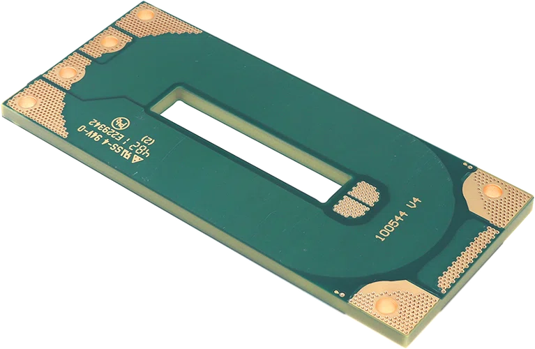
In the practical definition of the materials supply chain, these copper-based composite boards mainly evolve into two completely different physical forms: Heavy Copper PCBs (High Current Thick Copper PCBs): Their outer or inner copper foil thickness is typically greater than 3 ounces (105 micrometers). In extreme industrial-grade inverters or photovoltaic grid-connected DC-DC converters, the copper thickness can even soar to 10 ounces (350 micrometers) or even 20 ounces. This structure, almost entirely composed of heavy copper stacking, focuses on solving the electrical requirements of carrying hundreds of amperes of current in an ultra-small cross-sectional area.
Metal Core PCBs (Copper Base): Its core physical support is a solid pure copper metal plate, typically between 0.8 mm and 3.0 mm thick. On top of this, a copper conductor layer is attached through an extremely thin, highly thermally conductive insulating dielectric laminate. This structure does not participate in electrical conductivity; instead, it utilizes the exceptional thermal conductivity of pure copper, far exceeding the 237 W/(m·K) of the aluminum substrate, acting as a “high-speed heat pump” in three-dimensional space. However, this robust heterogeneous combination has been accompanied by intense internal micromechanical challenges from the outset.
The linear coefficient of thermal expansion (CTE) of pure copper is approximately 16.5 ppmC, while the CTE of the epoxy resin or ceramic-modified insulating layer above it is typically quite different. When this metal composite substrate undergoes lead-free reflow soldering at 260 degrees Celsius, or extreme high and low temperature thermal shock cycling in a car engine compartment ranging from -40 degrees Celsius to 150 degrees Celsius, the severe mismatch in the rates of thermal expansion and contraction between the copper and the insulating layer generates extremely high microscopic shear stress at the interface.
If the PCB manufacturer does not perform nanoscale chemical roughening of the copper surface before lamination (such as introducing an organic acid-micro-etching browning process to create countless microscopic honeycomb-like barbed structures on the copper surface), then under continuous cold shrinkage stress, catastrophic interlayer tearing and delamination will occur inside the substrate, causing the entire power motherboard to physically shatter without warning.
Molecular-level tuning of the thermal insulating layer (TIM): Dancing on the edge of the physical cliff between insulation and thermal conductivity. In the three-dimensional structure of the heat sink metal-based PCB, the core bottleneck that holds the entire system’s heat dissipation back is definitely not the thick copper base, but the thermal insulating layer (Dielectric Layer), only tens of micrometers thick, sandwiched between the copper conductors and the copper base. This dielectric layer faces a terribly paradoxical situation in physics: electrically, it must possess an extremely high dielectric breakdown voltage (typically above 4KV) to prevent the hundreds of volts of high voltage above from leaking to the pure copper substrate below; thermally, it must minimize thermal resistance to allow heat to conduct freely.
To achieve a balance on this physical precipice between insulation and thermal conductivity, top-tier substrate suppliers must perform molecular-level inorganic composite modification of the resin. Scientists are forcibly filling the traditional epoxy resin matrix with surface-modified nanoscale ceramic particles—such as aluminum nitride (AlN, with a thermal conductivity exceeding 200 W/(m·K)) or alumina (Al₂O₃) microcrystals—at a very high volume percentage (typically exceeding 60%). These nano-ceramic particles, through close physical contact within the resin, construct high-speed channels at the microscopic level specifically for phonon transport, forcibly increasing the overall thermal conductivity of the dielectric layer from a paltry 0.25 W/(m·K) to 3.0 W/(m·K), or even above 8.0 W/(m·K).
During manufacturing, PCB manufacturers must precisely control the heating rate and vacuum level of the hot press to ensure that these nano-ceramic particles are extremely uniformly distributed during resin curing. Localized resin-rich areas (which can cause localized thermal resistance spikes and chip burnout) or ceramic particle agglomeration areas (which can lead to localized dielectric strength collapse and high-voltage breakdown flashover) must be strictly avoided.
The Process Hell of Thick Copper Etching and Chemical Mechanical Polishing: Combating “Mushroom Heads” and Electrical Short Circuits.
When a heavy copper PCB board with a thickness of up to 6 ounces (210 micrometers) flows onto the production line, traditional PCB etching workshops often face a catastrophic chemical and mechanical battle.
The collapse of the etch factor and the geometry of “mushroom head” lateral etching: In standard PCB subtractive etching processes, a strong acidic copper chloride (CuCl2) solution is sprayed in a fan shape onto the copper-clad laminate surface through a high-pressure nozzle. For a typical 1-ounce (35-micron) substrate, the solution penetrates the copper layer vertically downwards extremely quickly, and lateral under-cut is almost negligible. However, when the copper thickness increases dramatically to 6 ounces or even higher, the etching solution takes several times longer to vertically penetrate this “copper wall.”
During this long chemical reaction window, the sidewalls of the conductors, already cut by the acid, are constantly exposed to the lateral immersion of the solution. This leads to an extremely serious physical consequence: the strong acid aggressively dissolves and hollows out the dry film (photoresist) laterally on both sides. When etching finally reaches the bottom insulating substrate, the conductor cross-section, which should have been a perfect rectangle, has been horizontally acid-etched into an extremely bizarre “inverted trapezoid” or a “mushroom shape” with a sharp, protruding top.
In materials science, this means a devastating drop in the etching factor. This mushroom-shaped structure is an absolute deadly hidden bomb during subsequent multilayer lamination or solder mask coating. Due to the severe geometric concavity at the mushroom-shaped edge, the high-viscosity solder mask ink cannot flow under that microscopic “eaves” during screen printing, thus locking an entire microscopic air tunnel at the conductor root. During subsequent high-temperature wave soldering during customer assembly, the trace moisture within this air tunnel vaporizes upon heating, generating a terrifying mechanical explosive force that directly lifts and peels off the solder mask layer in sheets. More seriously, under prolonged high-voltage operation, the sharp edges of two adjacent mushroom-shaped etching substrates can easily and instantly break down the air medium due to the tip discharge effect, triggering an irreversible high-current arcing short circuit on the board surface, rendering the entire inverter system of the new energy vehicle unusable on the spot.
To overcome the physical curse of the “mushroom-shaped” etching, high-end thick copper production lines must completely reconstruct the traditional single-pass fast-forward etching process, instead introducing multi-stage stepped high-vacuum etching and dynamic pattern compensation (Artwork Compensation) technology. In the CAM (Computer-Aided Manufacturing) stage, process engineers must perform a large-scale “pre-expansion compensation” on the photolithography black film or LDI laser data based on the specific tonnage of copper thickness—intentionally thickening the linewidth data to provide sufficient bite material for chemical dissolution during lateral etching. In actual processing, the substrate is sent to a high-end etching machine equipped with vacuum adsorption and directional spraying.
This equipment can instantly remove old etching waste liquid accumulated in the conductor grooves using high-pressure vacuum, ensuring that fresh, high-redox-potential copper chloride solution maintains its downward-firing kinetic energy, forcibly suppressing lateral diffusion to a minimum. After etching, the motherboard undergoes an extremely demanding chemical mechanical polishing (CMP) and stepped micro-etching process. High-density rotating brushes combined with a gentle complexing micro-etching agent physically smooth and micro-rounding the edges of the remaining “mushroom head” at the top of the traces. Through this high-cost process, the taper angle of traces weighing 6 ounces or more must be strictly controlled above 80 degrees, ensuring a stable base and smooth, rounded edges, creating an absolutely flat micro-geometric channel for 100% perfect filling of the subsequent solder mask.
Pushing the Limits of Heat Flux Density: Thermoelectric Separation and Embedded Copper Technology.
As high-power on-board chargers (OBCs), high-power lasers, and power amplifiers (PAs) race towards kilowatt levels, even with high thermal conductivity insulating metal substrates filled with nano-ceramic materials, the inherent slight thermal resistance of the dielectric layer remains a critical barrier to heat flow. To completely overcome this thermal resistance ceiling, top-tier high-power substrates have evolved the ultimate manufacturing process—thermoelectric separation and embedded copper coin technology.
Destroying Thermal Resistance: Placing Chip Pads Directly on a “Pure Copper Throne” The underlying logic of thermoelectric separation technology is extremely ruthless and efficient: Since the insulating dielectric layer conducts heat slowly, in the vertical projection area directly beneath core high-heat-generating components (such as MOSFET power transistors or laser chips), process engineers use high-precision depth-controlled milling cutters or CNC lasers to directly remove the epoxy resin and insulating dielectric layer inside the motherboard, creating a precise physical cavity. Subsequently, a solid copper block (Copper Coin), precisely machined at the micron level and perfectly sized, is embedded directly into this motherboard cavity using high-tonnage cold pressing or ultrasonic solid-state welding technology.
After surface electroplating, the top surface of this embedded pure copper block is completely flush with the outer conductive pads of the motherboard, forming an exposed metal plane; its bottom surface penetrates the entire board, completely exposed on the back of the motherboard, directly contacting the external giant aluminum liquid cooler through thermal paste. In this way, the base pads of the heat-generating chip are actually connected to the external cold source through a one-to-one, unobstructed, pure metal direct heat transfer via this solid red copper block. During conduction, heat instantly bypasses all insulating resin and thermally resistive media, resulting in a direct order-of-magnitude increase in heat dissipation efficiency. This forcibly lowers the junction temperature of the entire system by 20 to 30 degrees Celsius, creating an absolutely safe physical oasis for the high-frequency, full-load operation of high-power semiconductor devices.
While the direct-buried pure copper block technology is thermodynamically perfect, it plunges PCB manufacturers into a “sealed war” highly prone to short-circuit defects in terms of mechanical and chemical processing. Due to the difference in material rigidity, a microscopic boundary gap between the solid copper block and the surrounding milled FR4 resin substrate inevitably remains at their interface after mechanical bonding, with a width ranging from 10 to 30 micrometers. In subsequent multilayer lamination or surface chemical electroless gold plating (ENIG) processes, this microscopic gap becomes an extremely greedy “reservoir” of chemicals.
Highly penetrating chemical palladium activating solution and chemical nickel-gold plating solution will frantically penetrate into the motherboard through this tiny gap, becoming firmly locked within the resin fiber structure deep within. If the board manufacturer’s cleaning process is incomplete, these residual active metal ions will trigger a micro-electroplating effect in situ under a high-voltage, high-electric field when the motherboard is powered on. This will cause filamentous conductive metal channels to grow along the perimeter within the gap, directly leading to a localized high-voltage breakdown and short circuit between the surface signal conductors, which should maintain absolute electrical isolation, and the underlying pure copper heat sink. To seal this gap, the process necessitates the introduction of a unique high-flowability resin sludge plugging technique and a secondary micro-scrubbing control process.
After the pure copper block is embedded, a specially formulated high-modulus, high-filler, and extremely low-flow-shrinkage prepreg (PP) is used in a vacuum press for secondary overflow compaction. This forces the molten resin to completely fill the microscopic boundary gap under tens of atmospheres of pressure, followed by a high-temperature, full cross-linking and curing process lasting up to 4 hours. Subsequently, precision chemical mechanical polishing (CMP) is used to thoroughly cut and scrape away any excess residue on the surface, thus constructing a seamless, airtight physical barrier with extremely high dielectric strength between the pure copper block and the resin, completely eliminating any possibility of high-voltage leakage.
The Central Hub of Profits Amidst the Global Industrial and New Energy Red Ocean: High-Specification Flexible Industrial NPI Supply Chain Strategy.
With the global automotive industry’s full-scale transformation towards 800V high-voltage ultra-fast charging architecture and industrial energy storage inverters frequently reaching ultra-high power densities of hundreds of kilowatts, the demand for thick copper plates and copper-based substrates is experiencing explosive growth. However, due to the special processing involving high tonnage and large metal volumes, conventional printed circuit board (PCB) supply chains have erected numerous extremely troublesome barriers.
The “equipment gaps” and “long development cycles” of traditional supply chains pose significant challenges. In the current PCB manufacturing industry, thick copper and pure copper-based substrates are considered “special and scarce processes” with high profits but extremely capital-intensive processes. Ordinary digital or consumer electronics PCB manufacturers have in-house electroplating tanks with extremely low current densities, making it impossible to electroplat more than 3 ounces of thick copper within a reasonable timeframe. Furthermore, their existing etching lines would instantly paralyze and render the entire production line unusable if heavy copper plates were to be plated. This has led to the industry being almost entirely controlled by a few monopolistic, long-established listed giants that focus on heavy industry control, and are capable of producing copper substrates for new energy vehicle OBCs and high-power industrial power supplies.
While enjoying technological monopolies, these large manufacturers have also created an extremely challenging supply chain experience for global automotive Tier-1 R&D teams and agile industrial innovators. Due to the extremely low versatility of specialty materials (such as ultra-high thermal conductivity ceramic dielectrics and thick copper-clad laminates), these large suppliers typically do not maintain regular inventory. Once small-batch prototyping begins, the order scheduling cycle is often extended to 4 to 6 weeks or more because individual adjustments to the electroplating bath current and reconfiguration of the etching line speed are required. At critical junctures in automotive R&D or industrial power supply development where board modifications are urgently needed for performance testing and prototyping, a material delivery delay of over a month can completely disrupt the entire project team’s development rhythm, allowing competitors to ruthlessly overtake a previously leading market position within the delivery timeframe.
To unleash the innovative potential of heavy industry, leading process service providers, leveraging their long-term reserves of a full range of ultra-high thermal conductivity (3W to 8W/m·K) specialty copper-clad laminate raw materials and equipped with dedicated high charge current density vertical continuous plating lines (Heavy-Copper VCP) and vacuum controlled depth milling machines, must extend their capabilities in processing specialty thick copper to the R&D and small-batch stages: True Zero MOQ: Whether it’s 4-ounce to 15-ounce thick copper sheets or thermoelectric separation boards with directly embedded red copper blocks, there should be no minimum order quantity (MOQ) requirement in the early stages of R&D; a one-to-one automotive-grade Design for Manufacturability (DFM) process pre-review is mandatory.
Lightning-fast Delivery: Thanks to independent specialty plating and vacuum fast etching production lines, the prototyping cycle for specialty copper substrates and thick copper sheets, which often takes a month, can be compressed to within a few days through digital scheduling. An impeccable automotive-grade reliability white paper: Every high-specification copper PCB board leaving the factory must undergo 100% high-voltage insulation withstand voltage breakdown test (Hi-Pot Test), metallographic microsection analysis to prove that the copper conductor etching factor is greater than 3.5 and there are no “mushroom head” air gaps, and physical performance tests to ensure no delamination after three 288-degree hot float soldering tests. Ironclad factory test data ensures that every substrate can exhibit steel-like electrical stability in the extreme environment of high voltage and high current in new energy.