Stencil design is central to ensuring the quality of SMT printing; however, in practice, three key issues frequently arise: deviations in aperture design, defects in the substrate and manufacturing process, and defects in auxiliary structures. Negligence in any of these areas can lead to soldering defects and financial losses during mass production.
Three Major Categories of Core Defects in SMT Stencil Design
Deviations in Aperture Design
Apertures are key to the precise alignment between the stencil and PCB pads, and they are also the stage most prone to problems. Deviations directly result in abnormal solder paste volume, which in turn leads to various soldering defects. Among defects in SMT stencil aperture design, dimensional deviations are the most common.
When the length or width of the aperture does not match the pad, an oversized aperture results in excessive solder paste, causing issues such as bridging and solder balls; conversely, an undersized aperture leads to insufficient solder paste, resulting in cold solder joints or false soldering. For instance, if the aperture for a 0402-package component is reduced by just 0.1 mm from the standard, the cold solder joint rate can rise directly to over 15%.
In addition to dimensional deviations, unreasonable aperture shapes must not be overlooked. Using circular apertures for square pads can easily lead to uneven solder paste distribution, affecting the formation of solder joints; meanwhile, apertures for densely packed pins (such as QFP packages) without anti-bridging design can result in a bridging defect rate of up to 20%.
Furthermore, misalignment and disproportionate dimensions of apertures also pose risks. When the deviation between the aperture centre and the pad centre exceeds 0.05 mm, it affects component placement accuracy; if the aperture’s ‘width-to-height ratio’ is less than 1.5 or the ‘area ratio’ is less than 0.6, it leads to poor solder paste release, and residual solder paste may affect subsequent printing processes, increasing production risks.
Substrate and Process Defects
The quality of the stencil substrate and the manufacturing process determine its structural stability and service life, and are often overlooked as potential sources of hidden defects. Currently, stainless steel is the most commonly used substrate in the industry, with a typical thickness of 0.1–0.2 mm. If local thickness deviations exceed 0.02 mm, this will cause fluctuations in solder paste volume in the corresponding areas. This impact is particularly significant for micro-components such as 01005, and may even directly lead to batch product defects.
Tension control is a core requirement of the stencil process. Once properly tensioned, the stencil’s tension should be maintained at 30–50 N/cm². Insufficient tension can cause the stencil to deform during printing, resulting in distorted solder paste patterns; uneven tension, in turn, leads to inconsistent local printing pressure, causing variations in solder paste volume and indirectly increasing the rate of soldering defects.
Furthermore, if burrs exceeding 0.01 mm are present on the edges of apertures created by laser cutting or chemical etching, they may scratch the PCB surface or leave solder paste residue; if the four corners of the stencil become deformed due to improper installation, this will result in a poor seal against the PCB during printing, causing missed prints and affecting production continuity.
Defects in the Auxiliary Structure
Although the auxiliary structure of the stencil does not directly participate in solder paste application, it does affect production compatibility and ease of operation; defects in this structure can similarly trigger a cascade of problems. Misalignment of the positioning holes is a common defect in the auxiliary structure. If the clearance between the stencil’s positioning holes and the printer’s positioning pins exceeds 0.03 mm, this will cause the stencil to shift during printing, resulting in misalignment between the solder paste pattern and the pads, which in turn affects the quality of subsequent component placement and soldering.
Unsuitable frame design can also cause numerous problems. Insufficient frame strength may lead to warping after the stencil is installed, affecting printing flatness; insufficient clearance between the frame and the PCB may damage edge components or the solder mask, resulting in product wastage. These seemingly minor defects in the auxiliary structure often impact production efficiency and increase rework costs for the company, and therefore require close attention.
To address various defects in stencil design, there is no need for complex equipment. By employing a three-step approach of ‘visual inspection + physical testing + trial printing verification’, issues can be quickly identified, providing precise data for subsequent optimisation. This method balances inspection efficiency and accuracy, meeting the needs of PCB manufacturers for mass production.
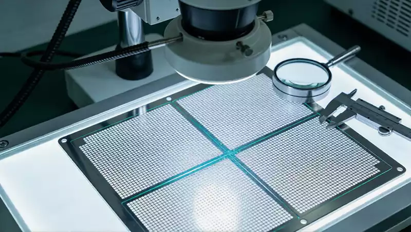
Visual inspection, as the core step in the initial screening process, enables rapid identification of surface defects. Using a high-intensity desk lamp and a 10–20x magnifying glass, the focus is on checking whether the edges of the apertures are smooth and free from burrs or deformation; whether the stencil surface has scratches, stains or signs of corrosion; whether the frame is securely attached to the mesh and free from warping; and whether the registration holes are intact, free from wear, and consistent in diameter with the design.
Building on this, the stencil is placed on a light-transmitting platform and superimposed over the PCB design drawing (or a printed copy of the CAD file). Through light transmission comparison, it is confirmed whether the deviation between the aperture positions and the pad positions is within 0.05 mm, whether the aperture shape and dimensions match the drawing, and whether the spacing between apertures in dense areas complies with anti-bridging design requirements.
Physical testing is used to quantitatively verify the structural stability of the stencil, compensating for the limitations of visual inspection. For tension testing, a stencil tension gauge is used to select nine test points evenly distributed across the stencil surface (in a 3×3 matrix). After measurement, the average value and deviation are calculated.
If the average value is below 30 N/cm², this indicates insufficient tension and the stencil must be retensioned; if the deviation of any single point from the average exceeds 10%, this indicates uneven tension and the tensioning mechanism must be adjusted.
Thickness testing employs a micrometer with an accuracy of 0.001 mm to measure 10 points across different areas, including the stencil edges, centre and around the apertures. A deviation exceeding 0.02 mm is deemed to indicate uneven thickness. For positioning accuracy testing, the stencil is mounted on the printing machine, and a CCD vision system is used to compare the coordinate deviations between the stencil’s registration holes and the PCB’s registration holes; any deviation exceeding 0.03 mm requires immediate correction of the registration hole positions.
A test print is the final verification step simulating production and is also the most direct method for identifying defects. Select 1–2 test PCBs and print them using standard production parameters (printing speed 20–40 mm/s, pressure 5–10 N, de-sticking speed 1–3 mm/s). Combine this with solder paste inspection (SPI) to pinpoint issues accurately.
After printing, visually inspect the solder paste patterns for any missed printing, missing corners (which may be caused by blocked apertures or insufficient tension), bridging, solder balls (which may be caused by excessively large apertures or unreasonable shapes), and whether the solder paste is centred on the pad (to determine aperture position deviation); Use SPI equipment to measure the height, volume and area of the solder paste. If the volume deviation exceeds ±15%, this may indicate issues with the aperture dimensions or stencil thickness; if the height is uneven, check whether the stencil tension or printing pressure is consistent.
Optimisation of Via Design
The core principles of via design are ‘alignment with the pad and facilitating solder paste release’, which require precise adjustment based on component type and pad dimensions. For surface-mount components (0402 and larger), the via width should be set at 0.9–1.0 times the pad width, and the length at 0.85–0.95 times the pad length; this ensures the solder paste is centred whilst preventing overflow.
For components with dense pin arrangements, such as QFPs and BGAs, reducing the aperture dimensions by 0.05–0.1 mm compared to the pads can effectively prevent bridging; for 0.5 mm pitch QFPs, the aperture spacing must be no less than 0.1 mm. For large pads, such as those on connectors, ‘grid-like’ or ‘strip-shaped’ apertures are used to improve release properties and prevent solder paste residue.
Shape optimisation is equally critical; for square pads, using “rounded-corner rectangular” apertures reduces edge stress and lowers the risk of burr formation; in high-density pin areas, anti-bridging apertures should be employed, such as adding isolation bars between pins or using “teardrop-shaped” apertures, to further optimise release performance.
Regarding positional alignment, by comparing the coordinates of CAD files with the stencil aperture data, laser correction equipment is used to adjust misaligned apertures, ensuring deviations do not exceed 0.03 mm and improving matching accuracy.
Substrate and Process Optimisation
Substrate selection must align with production requirements; for micro-components (01005), 0.1 mm thick ultra-fine stainless steel mesh is prioritised to ensure flatness deviations do not exceed 0.01 mm; The edges of the laser-cut apertures undergo passivation to remove burrs, ensuring a surface roughness (Ra) of no more than 0.8 μm; coating the stencil surface with nickel or Teflon reduces solder paste adhesion, improves release properties, and extends the stencil’s service life.
Tension optimisation employs the ‘four-point uniform tensioning method’ to ensure tension fluctuations do not exceed 5 N/cm²; After tensioning, the stencil is left to rest for 24 hours before aperture processing to relieve residual stress and prevent deformation during subsequent use. Regarding edge treatment, deformed stencils are repaired using a flatness correction machine to ensure surface flatness does not exceed 0.02 mm; where burrs on aperture edges exceed 0.01 mm, they are removed via secondary chemical etching or manual grinding to prevent scratching of the PCB or residual solder paste.
Optimisation of Auxiliary Structures and Production Adaptation
Optimisation of positioning holes employs a ‘stepped hole’ design to accommodate pins of varying diameters, with hole diameter tolerances controlled to ±0.01 mm; severely worn positioning holes are repaired by reaming and inserting copper sleeves to ensure a clearance of no more than 0.02 mm, thereby enhancing positioning accuracy.
For the frame design, aluminium alloy with a thickness of no less than 5 mm is selected to balance strength and lightweight construction; The clearance between the frame and the PCB board is no less than 2 mm. For PCBs with components at the edges, clearance notches are added at the corresponding positions on the frame to prevent damage to components or the solder mask.
If the stencil design itself has no obvious defects but poor demoulding occurs during test printing, this can be addressed by adjusting the printing parameters: reduce the printing speed to 15–25 mm/s to extend the solder paste filling time; increase the lift-off height to 2–4 mm and reduce the lift-off speed; appropriately increase the printing pressure (not exceeding 12 N) to ensure close contact between the stencil and the PCB, thereby improving solder paste printing quality.
Rapid inspection and optimisation are ‘after-the-fact remedies’; establishing a comprehensive quality control system is essential to reduce stencil design defects at source, achieve long-term cost reduction and efficiency gains, and is also key to PCB enterprises enhancing their core competitiveness.
Standardised design specifications form the foundation. Companies must establish a ‘Stencil Design Specification’ to define the aperture dimensions, shapes and proportional standards for different components, and create a ‘component-aperture’ database. Prior to design, DFM (Design for Manufacturability) software should be used to simulate the rationality of apertures, thereby avoiding potential design issues in advance.
Supplier management is equally important. Companies should select stencil suppliers with ISO 9001 certification and require them to provide material certificates, tensile strength test reports and aperture dimension inspection reports. Quarterly quality audits of suppliers should be conducted, and cooperation with suppliers whose defect rate exceeds 3% should be suspended to ensure the quality of stencils at source.
Stencil lifecycle management is indispensable. It is recommended that stencils be used no more than 5,000 times. After each use, wipe the surface with isopropyl alcohol and blow through the apertures with compressed air to remove any solder paste residue. Regularly (every 1,000 uses) re-test tension and aperture dimensions; stencils that fail to meet requirements should be scrapped or repaired promptly to prevent production defects caused by stencil ageing.
The quality of stencil design directly determines the success or failure of SMT printing. By systematically identifying three core defect categories and implementing precise optimisation through a combination of ‘visual inspection, physical testing and trial printing verification’, whilst establishing a comprehensive control system spanning from design specifications to lifecycle management, companies can effectively reduce printing defects at source, laying a solid foundation for subsequent placement and soldering processes.