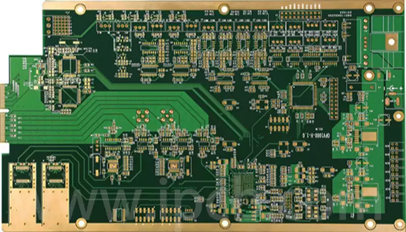
HDI PCB definition, High Density Interconnect Board, is a circuit board with high line distribution density using micro-blind/buried hole technology. It is able to achieve higher line density and finer wiring in limited space to meet the demand for miniaturisation, high performance and high reliability of modern electronic products.
In the field of pcb board, HDI mainly refers to the interconnection technology between the pads and components of the hdi PCB, i.e., by introducing more electrical vias inside the board layer, the wiring distance between the pads of the components and their driver pins is much closer, through which we can integrate more electronic components under the same area, making the equipment more compact and more efficient.
Types of hdi boards
HDI boards are divided into the following four main types, each with its own unique structure and application scenarios:
- First-order HDI boards
First-order HDI boards are the most basic HDI designs and usually contain only two layers of circuitry (top and bottom) and one type of connection – blind vias. Blind vias connect only some of the board’s surface layers to the inner layers and do not run through the entire board. First-order HDI boards are often used for low-density connections and low-complexity applications, and are suitable for cost-sensitive products or circuit designs with low functionality requirements. - Second Order HDI Boards
Second order HDI boards contain more layers, typically two layers of circuitry and a buried vias layer. The buried vias connect the two or more layers of circuitry inside the board. Second-order designs can provide higher circuit density than first-order designs and are suitable for medium-complexity circuits, especially in smartphones, tablets, and consumer electronics devices. - Third-order HDI boards
Third-order HDI boards typically feature three and more layers of circuitry and more complex connections, including blind vias, buried vias, and microvias. Third-order designs enable higher circuit densities in a smaller space, and are suitable for the design of multi-layer complex circuits, such as 5G communications, complex consumer electronics, medical devices, and automotive electronics. - Anylayer HDI Boards
Anylayer HDI boards are a more advanced HDI design that enables connections between any layers, not just between surface and inner layers. This design provides greater flexibility and higher circuit density for board designs that require extremely high density and complex functionality. The current Anylayer HDI that is more commonly used in electronic end products is 10 or 12 layers.
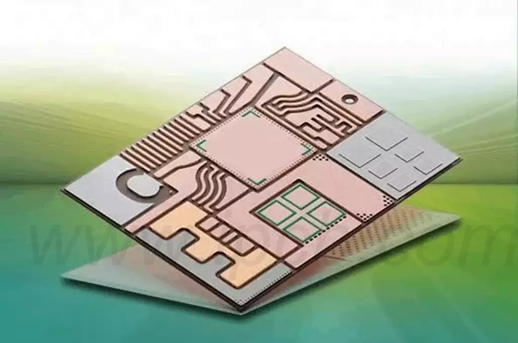
The main difference between thin HDI PCBs and conventional PCBs is their higher wiring density and more compact structure. The boards are connected to the different circuit layers by means of laser drilling techniques to achieve tiny through-holes (typically less than 150 microns in diameter), as well as by using blind and buried vias. These tiny connections help to significantly increase the density of circuits per unit area, enabling designers to integrate more functionality in a limited space.
The main difference between thin HDI PCBs and conventional PCBs is their higher wiring density and more compact construction. The boards are connected to the different circuit layers by means of laser drilling techniques to achieve tiny through-holes (typically less than 150 microns in diameter), as well as by using blind and buried vias. These tiny connections help to significantly increase the density of circuits per unit area, enabling designers to integrate more functionality in a limited space.
The dielectric layers of thin HDI PCBs are typically very thin, e.g., 80 microns or less, and need to be uniformly thick, which is especially important for impedance-controlled, high-density boards. This thin design not only enables more compact products, but also significantly improves electrical performance. Shorter signal paths and advanced cabling techniques reduce signal attenuation, crosstalk and signal loss, ensuring signal integrity and reliability for high-speed data transmission. Additionally, HDI PCBs often feature lead-free solder, which is safer for workers and consumers and reduces the environmental footprint. While the initial cost may be higher, HDI PCBs reduce the total cost of ownership in the long run by reducing the number of materials and layers and improving long-term reliability.
Thin HDI PCBs typically have a thinner dielectric layer thickness. Specific dielectric thicknesses vary depending on the design and application:
General Range: Dielectric thicknesses for HDI circuit boards are typically less than 80 microns (um) and require greater thickness uniformity, especially on high density boards and package substrates that require characteristic impedance control.
Mainstream Choice: As the trend toward device miniaturisation continues, 0.1 mm (100 micron) dielectric layers have become the mainstream choice for HDI boards.
Specific Design Examples: In some board designs with ultra-thin dielectric layers, the thickness of the intermediate dielectric layer can be 64 microns, and the other dielectric layers can be 46 microns or 35 microns thick. The thickness of the dielectric layer can be designed to be 25 ± 5 microns, while the thickness of the outermost dielectric layer is 31 microns. The thickness of the solder-resistant layer is typically 10 microns.
Prior art example: In the design of an existing 10-layer board for a smartphone, a 0.064 mm FR4 substrate is used for the fifth dielectric layer, 1080 semi-cured sheets are used for the rest of the dielectric layers (with thicknesses of 0.08 mm and 0.07 mm, respectively), and the first and tenth dielectric layers have a thickness of 0.035 mm, while the rest of the layers have a thickness of 0.03 mm, for a total thickness of 1,034 micrometres in the finished board.
Ultra-thin dielectrics: Through-hole diameters as low as 5 µm can be achieved in dielectrics with a thickness of 5 µm by laser drilling techniques. Accumulated dielectric layers are typically used in conjunction with thin core layers with thicknesses as low as 2 mils (approximately 50.8 microns). The thinner the dielectric layer, the finer the lines and spacing can be made.
HDI PCB cost composition mainly contains the following aspects:
- Material Costs: Materials used in the production of HDI PCB includes copper-clad laminates, filler materials, resins, induced materials, and encapsulation materials. As HDI PCBs usually require the use of higher specification substrates and more complex insulating materials, their material costs are relatively high compared to traditional PCBs.
- Processing costs: The production of HDI PCB involves multiple processes, such as microvia drilling, blind and buried hole processing, surface treatment, lamination and lamination. Each process requires specialised equipment and technology, increasing processing costs.
- Equipment investment: The production of HDI PCB requires high-precision equipment, such as laser drilling machines and precision printing machines, which are usually expensive and costly to maintain. Therefore, equipment investment is an important cost component.
- R&D costs: As the design and production process of HDI PCB is more complex, companies need to invest a lot of R&D resources in the development of new technologies and process optimisation, which will also affect the overall cost.
- Labour costs: HDI PCB production process technicians and operators need to have higher skills, so labour costs are relatively high.
- Inspection and testing costs: HDI PCB in the production process requires a number of quality inspection and testing to ensure product performance and reliability, which also increases the cost.