IC packaging involves encapsulating the bare die—cut from a wafer—into a complete component that can be directly mounted onto a PCB. It fulfils three fundamental functions: establishing an electrical connection between the die and external circuits, protecting the die from environmental damage, and aiding heat dissipation.
To give a practical example: in the case of a mobile phone processor chip, the bare die measures only a few square millimetres; it is fragile and cannot be soldered directly. Through packaging technology, which involves the addition of leads and a protective casing, the die can be securely mounted on the mobile phone’s motherboard to facilitate signal transmission and heat dissipation. Without packaging, even the most advanced chips cannot be put into practical use.
The Three Key Functions of IC Packaging
Electrical Connection
Connecting the solder pads on the die to the package leads enables the chip to communicate with other components on the PCB. This is the most fundamental function of packaging and one of the core challenges in its design.
Physical Protection
The bare die is extremely sensitive to moisture, dust and temperature fluctuations. The package housing isolates it from the external environment, preventing damage. This is also why industrial-grade and automotive-grade chips have more stringent packaging requirements.
Heat Dissipation
Chip operation inevitably generates heat. The packaging materials and structure must effectively conduct this heat to the PCB or heat sink to prevent overheating, throttling or even burnout. For high-frequency chips, thermal management is often the primary consideration in packaging design.
The Core Structure of IC Packaging
A basic IC package primarily consists of three parts: the die, the package substrate, and the leads and encapsulant. Among these, the package substrate acts as a ‘bridge’—connecting the die to the PCB. Its material and routing precision directly affect signal transmission efficiency.
Many engineers overlook the dielectric constant of the package substrate. Particularly in high-frequency applications, an inappropriate choice of substrate material can lead to signal attenuation and increased crosstalk. I once encountered a pitfall in a 5G module project: due to the use of a standard FR-4 substrate, signal loss far exceeded the specified limits; the issue was only resolved after switching to a high-frequency substrate.
IC Packaging Types
1.DIP Packaging (Dual In-Line Package)
The most classic and fundamental packaging type, with pins extending from both sides and using through-hole soldering.
Advantages: Low cost, simple soldering.
Disadvantages: Low pin density, average heat dissipation.
Applications: Low-end microcontrollers, power management chips, and other scenarios with low performance requirements (such as home appliance control boards and simple sensor modules). It is gradually being phased out in new designs, but remains widely used in the industrial control sector.
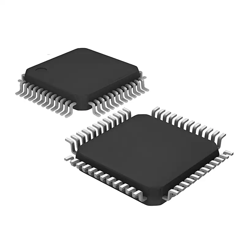
2.SMD Packaging (Surface Mount Device)
Currently the most widely used packaging type, with pins located on the bottom or sides of the package. It is suitable for automated assembly and offers a much higher pin density than DIP. Common sizes include 0402 and 0603, as well as high-density pin types such as QFP and QFN.
I would like to highlight the QFN package (Quad Flat No-lead package): this is my most frequently used choice in high-frequency projects—the leadless design reduces signal interference and offers superior heat dissipation compared to traditional solutions, making it highly suitable for applications with high performance requirements, such as RF chips and MCUs. However, special attention must be paid to pad design during soldering to prevent cold solder joints.
3.BGA Packaging (Ball Grid Array)
The pins are distributed in the form of solder balls on the underside of the package, enabling extremely high pin density. This is suitable for complex chips such as CPUs, FPGAs and high-end MCUs.
Advantages: Good signal integrity and excellent heat dissipation.
Disadvantages: High cost, and difficult to solder and repair.
Selection of IC Packaging Materials
1.Packaging Substrate Materials
Low-frequency applications (≤1GHz): Standard FR-4 substrates are sufficient; these are low-cost and easy to process, making them suitable for consumer electronics.
High-frequency applications (≥2GHz): High-frequency substrates (such as those made from Rogers or Tectrion high-frequency materials) must be used; these effectively reduce signal loss and are suitable for 5G and RF modules.
2.Encapsulant Materials
General applications: Epoxy resin, which is low-cost and offers good insulation.
High-temperature/high-reliability applications (automotive electronics, industrial control): Ceramic encapsulation, which is heat-resistant and offers strong immunity to interference, but is relatively expensive.
3.Lead Materials
Most applications: Copper leads, which offer good conductivity and are moderately priced.
High-end applications (aerospace, medical equipment): Gold leads, offering strong oxidation resistance and high reliability, but are expensive and should not be selected unless necessary.
Design tips: BGA packaging places high demands on PCB layout, requiring particular attention to thermal management and impedance matching. This is especially true for multilayer PCBs, where the stack-up structure directly affects both signal transmission and thermal dissipation in the BGA.
Three core principles for selecting IC packaging
Match the product application
Prioritise a balance between the three key factors: thermal management, size and cost. For example: automotive electronics should opt for high-temperature-resistant, high-reliability packages; whereas consumer products can strike a balance between cost and performance.
Consider Manufacturability
Do not blindly pursue high pin density. If the manufacturing process cannot meet soldering requirements, even the best package cannot be implemented. For instance, in small-batch production, avoid BGA where possible and choose SMD packages that are simpler to solder.
Allowing for Thermal Management
For high-frequency, high-power chips, thermal design must be considered simultaneously when selecting a ic packaging. Where necessary, choose packages with integrated heat sinks to avoid rework later due to thermal issues.
IC packaging is far more than simply ‘dressing’ a chip—it fulfils three key functions: electrical connection, physical protection and thermal conduction. It directly determines whether the bare die can perform reliably in the final product.