What is 5G millimetre wave? 5G millimetre wave, also known as the millimetre wave band, refers to the spectrum segment with wavelengths between 1mm and 10mm, corresponding to frequencies ranging from 30 to 300GHz. In practical applications, frequencies above 24GHz are classified as millimetre waves. This band occupies the overlapping wavelength range between microwaves and far-infrared waves, thereby exhibiting characteristics of both spectrum types. The theoretical and technological underpinnings of millimetre waves represent the extension of microwaves towards higher frequencies and the evolution of light waves towards lower frequencies.
Advantages of 5G Millimetre Wave (mmWave)
High Speed, High Capacity: Millimetre wave technology delivers exceptionally high data transmission speeds, with peak rates reaching 30Gbps. It supports simultaneous connections for a vast number of devices, making it ideal for scenarios such as high-definition video streaming and virtual reality.
Low Latency: By reducing communication delays, mmWave enables faster response times. This makes it highly suitable for applications requiring real-time data transmission, such as autonomous driving and remote control systems.
High Directivity: Millimetre wave exhibits strong directionality with narrow beams, facilitating precise positioning and transmission. This enhances signal security and minimises interference.
All-weather capability: Millimetre wave propagation is significantly less affected by weather conditions, offering all-weather functionality.
Millimetre wave also presents certain challenges, such as relatively high base station construction costs, limited signal coverage range, and susceptibility to obstruction by buildings and obstacles. Consequently, it is anticipated that millimetre wave will be deployed and integrated closely with Sub-6GHz 5G and 4G LTE to collectively ensure the performance and coverage of mobile wireless networks.
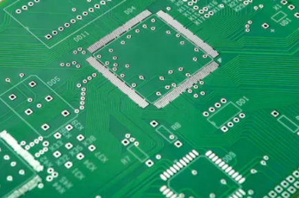
The advent of 5G millimetre wave (mmWave) communication technology heralds a new era of high-frequency, high-bandwidth communication systems. The mmWave spectrum, spanning frequencies from 24GHz to 100GHz, delivers data throughputs of several gigabits per second for 5G. However, as frequencies increase, traditional PCB design principles face significant challenges, particularly in the interconnect design of antenna substrates. The extremely short wavelengths of millimetre-wave signals (approximately 1–10 mm) impose unprecedented demands on signal integrity, parasitic effects, and manufacturing tolerances.
Analysing Millimetre-Wave Interconnection Challenges
Interconnection Losses and Parasitic Effects
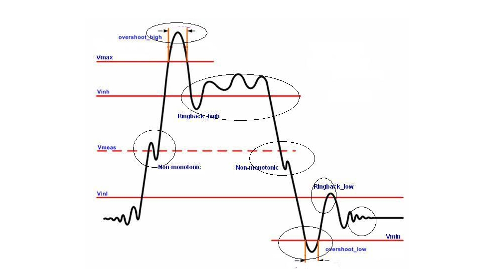
A core difficulty in millimetre-wave interconnections lies in their potential to become a primary source of signal loss. At these frequencies, any form of interconnection may significantly degrade signal integrity. Traditional through-holes or blind vias readily form parasitic inductance and capacitance at millimetre wave frequencies, leading to reflections and bandwidth degradation. Parasitic capacitance and inductance readily cause reflections and bandwidth loss. Furthermore, millimetre wave frequencies impose heightened demands on design elements such as pads and traces.
Manufacturing Tolerance Challenges
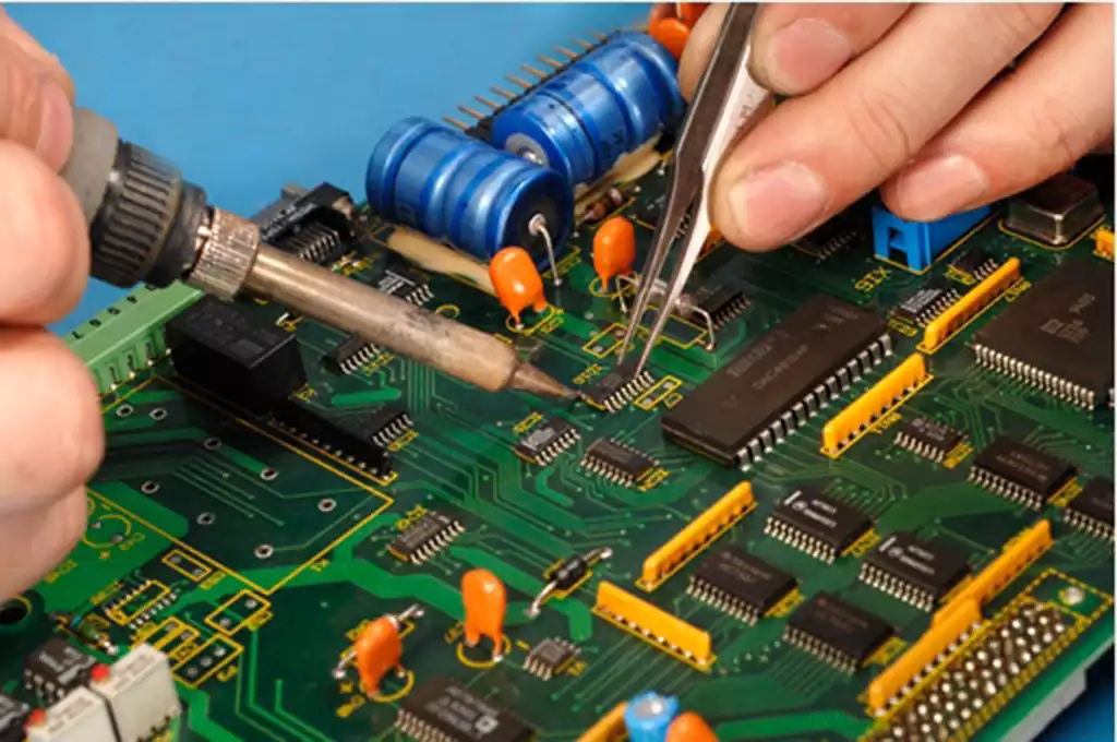
Millimetre-wave interconnects demand exceptionally high manufacturing precision, with their structural requirements far exceeding those of conventional microwave designs. Factors such as PCB layer-to-layer alignment deviations, variations in copper foil thickness, and dielectric constant inhomogeneities can all impact interconnect performance. Therefore, manufacturing tolerances must be thoroughly accounted for during the design phase. These challenges necessitate designers to consider potential deviations and inhomogeneities early in the design process to ensure the final product’s performance meets expectations.
The advent of 5G millimetre wave (mmWave) communication technology heralds a new era of high-frequency, high-bandwidth communication systems. The mmWave spectrum, spanning frequencies from 24GHz to 100GHz, delivers data throughputs of several gigabits per second for 5G. However, as frequencies increase, traditional PCB design principles face significant challenges, particularly in the interconnect design of antenna substrates. The extremely short wavelengths of millimetre-wave signals (approximately 1–10 mm) impose unprecedented demands on signal integrity, parasitic effects, and manufacturing tolerances.
Analysing Millimetre Wave Interconnection Challenges
Interconnection Losses and Parasitic Effects
A core difficulty in millimetre wave interconnections lies in their potential to become a primary source of signal loss. At these frequencies, any form of interconnection may significantly degrade signal integrity. Traditional through-holes or blind vias readily form parasitic inductance and capacitance at millimetre wave frequencies, leading to reflections and bandwidth degradation. Parasitic capacitance and inductance readily cause reflections and bandwidth loss. Furthermore, millimetre wave frequencies impose heightened demands on design elements such as pads and traces.
Manufacturing Tolerance Challenges
Millimetre-wave interconnects demand exceptionally high manufacturing precision, with their structural requirements far exceeding those of conventional microwave designs. Factors such as PCB layer-to-layer alignment deviations, variations in copper foil thickness, and dielectric constant inhomogeneities can all impact interconnect performance. Therefore, manufacturing tolerances must be thoroughly accounted for during the design phase. These challenges necessitate designers to consider potential deviations and inhomogeneities early in the design process to ensure the final product’s performance meets expectations.

5G Millimetre-Wave Interconnect Design Optimisation Strategies
- Optimising High-Frequency Signal Transmission
Material Selection: Employ low-loss PCB materials (e.g., PTFE) and air-dielectric connectors to minimise signal attenuation. For instance, SMP/SMPM connectors utilise PTFE dielectric material, balancing performance and cost.
Dimension and Tolerance Control: At high frequencies, connectors require smaller dimensions and tighter tolerances (e.g., 2.92mm connectors demand 2-3 times tighter tolerances than SMA connectors) to guarantee signal integrity. - Electromagnetic Compatibility (EMC) Management
Shielding Design: Reinforce shielding for board-to-board connectors and coaxial cables to mitigate electromagnetic interference (EMI) and crosstalk. For instance, slotted ground conductors require precise design to prevent axial misalignment of openings.
Layout Optimisation: In multilayer PCB designs, rationally plan signal and ground planes while employing via isolation techniques to reduce EMI risks. - Thermal Management and Reliability Enhancement
Heat Dissipation Design: Employ thin thermal interface materials (TIM) to optimise heat dissipation pathways and prevent localised overheating. For instance, NXP’s solution simplifies assembly through heat sink silicon interlayers while reducing TIM thermal resistance.
Structural Reinforcement: Limit PCB via count and adopt staggered via placement to counteract thermal expansion differences, thereby mitigating warpage risks. - Beamforming and Antenna Array Optimisation
Beam Management Technology: Employ hybrid digital-analogue beamforming combined with beam scanning and switching algorithms to enhance signal coverage and interference resistance.
Antenna Array Design: Utilise large-scale MIMO antenna arrays to boost signal strength through beamforming while reducing single-channel power requirements. - Automated Testing and Interconnect Solutions
Blind-Mate Connectors: Employ blind-mate coaxial connectors and spring-loaded probes to minimise manual intervention, improving test efficiency and repeatability.
Automated Assembly: Utilise robotic technology for connector insertion/removal and probe positioning, ensuring interconnect precision and reliability. - System-Level Co-Design
Electromagnetic-Circuit Co-Simulation: Integrates EM simulation with circuit modelling tools, automatically generating 3D finite element models to extract critical path electromagnetic characteristics, thereby shortening design cycles.
End-to-End Optimisation: Starting from system requirements, coordinates RF front-end, antenna array, and beam management stages to achieve performance-cost trade-offs.
5G millimetre wave technology delivers unprecedented high-speed and high-capacity communication capabilities, yet poses formidable challenges for interconnect design—particularly concerning high-frequency losses, parasitic effects, and manufacturing tolerances. These technical hurdles can be effectively addressed through low-loss materials, optimised dimensional tolerances, enhanced electromagnetic shielding, and precise thermal management, thereby safeguarding millimetre-wave signal integrity and system reliability.
As technology evolves, integrating advanced antenna array techniques such as beamforming and massive MIMO will significantly enhance 5G millimetre wave coverage and interference resistance. Automated testing and assembly strategies, including blind-mate connectors and robotic technology, will further improve the efficiency and precision of interconnect solutions. Concurrently, system-level co-design—encompassing electromagnetic-circuit co-simulation and end-to-end optimisation—will become pivotal in advancing millimetre-wave technology maturity.