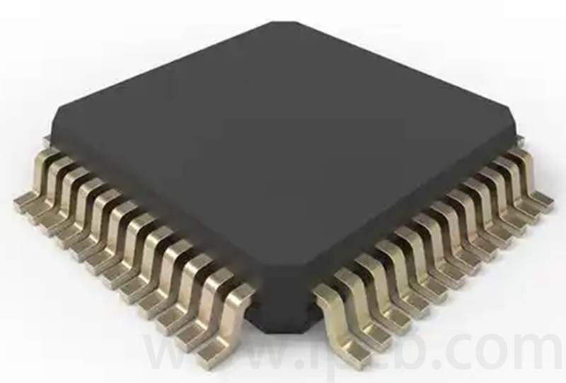
What is dual inline package? Dual inline package (DIP) is a type of integrated circuit package whose main feature is that the integrated circuit chip is mounted on two parallel rows of metal pins. This type of package is simple, easy to produce and maintain, so it is widely used in the electronics industry.
Dual in-line packages are usually used for electronic components to connect each component directly on the circuit board, thus improving the assembly efficiency of the circuit board. Through the design of dual in-line packages, the distance between components can be made closer, thus making the whole circuit board more compact and stable.
Features of DIP packages:
Package structure:
DIP packages have two parallel columns of pins, typically ranging from 8 to 64 pins, with a typical pin spacing of 2.54 mm (0.1 inch). This design allows components to be connected by inserting them into the appropriate holes on the printed circuit board (PCB).
Plug-in method:
DIP components are soldered to the other side of the PCB by inserting the pins directly into the reserved holes on the PCB. This type of insertion makes it relatively simple to solder or replace components, making it easy to repair and replace.
Wide range of applications:
DIP packages were initially widely used in integrated circuits (ICs) and logic chips, and are still widely used in various types of electronic devices, such as microcontrollers, operational amplifiers, memory and so on.
Size and Volume:
DIP packages are relatively large, making them less flexible than modern SMD (surface mount technology) packages in some compact designs. However, they are still popular for prototyping and education due to their simple structure and ease of hand soldering.
Thermal Performance:
DIP packages typically have better thermal performance and are suitable for some higher power applications.
THT uses components with leads, designed circuit connection wires and mounting holes on the printed circuit board, by inserting the component leads into the pre-drilled holes on the PCB, and then temporarily fixing them on the other side of the substrate using wave soldering and other soft brazing techniques to form a reliable soldering joint to establish a long-term mechanical and electrical connection, with the main body of the component and the soldering joints located on both sides of the substrate respectively. With this method, the problem of reducing the size cannot be solved after the circuit is densely packed to a certain extent because the components have leads. At the same time, it is difficult to eliminate faults caused by the proximity of the leads to each other and interference caused by the length of the leads.
DIP package (DualIn-linePackage) is a THT plug-in process in a part packaging technology, is one of the simplest packaging. The vast majority of small and medium-sized integrated circuits use this form of packaging, the number of pins is generally not more than 100.DIP package CPU chip has two rows of pins, need to be inserted into the chip socket with DIP structure.
DIP Production Flow
Component Forming and Processing
Before production begins, the staff in the preprocessing shop will collect the required components from the material warehouse according to the bill of materials (BOM) and carefully check the model and specifications. They then use automated equipment such as bulk capacitor trimmers, transistor auto-formers and fully automated tape formers to preform the components according to the production template. This step ensures that the component’s pin shape and dimensions are correct for subsequent insertion.
Insertion
The pre-processed components are inserted exactly into the corresponding holes on the finished PCB. This is in preparation for the wave soldering process.
Wave soldering
The inserted PCBs are placed on the conveyor belt of the wave soldering machine. The process includes fluxing, preheating, soldering through the wave formed by the liquid solder, and finally cooling. Wave soldering is a critical step in the DIP production process, as it connects the components to the PCB by means of a wave of molten liquid solder.
Component Cutting
The soldered PCBA board needs to be cut to ensure that the length of the component pins meets the specified dimensions.
Patch welding (post-soldering)
During the quality inspection process, if it is found that there are areas of the finished PCBA board that are not fully welded, manual patch welding and repair is required to ensure the integrity of the weld.
Cleaning
In order to achieve the environmental standards and cleanliness required by the customer, the residual flux or other harmful substances on the finished PCBA board must be thoroughly cleaned.
Functional Test
The finished PCBA board is functionally tested after component soldering and cleaning. This step is to verify that the PCBA board functions properly. If the test found any functional defects, need to be repaired and re-tested until the product meets the qualification standards.
The DIP production process can be divided into component moulding. Insertion. Wave soldering. Components cut (cut) feet. Soldering. Wash board and function test seven steps:
- Pre-processing of components. First of all, pre-processing workshop staff according to the bill of materials to the material to receive materials, carefully check the material type. Specification, sign, according to the sample plate for pre-production processing, the use of automatic bulk capacitor foot cutting machine. Automatic crystal moulding machine. Automatic belt moulding machine and other moulding equipment for processing;
- Insertion, the patch processing of good components inserted into the corresponding position of the PCB board, in preparation for the wave soldering;
- Wave soldering, the plug-in good PCB board into the wave soldering conveyor belt, after spraying flux. Preheat. Wave soldering. Cooling and other links to complete the welding of the PCB board;
- Component cutting (shear) feet, the completion of the welding PCBA board for cutting (shear) feet to achieve the appropriate size;
- Mending welding (post-soldering), for checking out the finished PCBA board is not welded complete to make up for the welding, repair;
- Wash the board, residual flux and other harmful substances on the PCBA finished product to clean, in order to achieve the environmental standards required by the customer cleanliness;
- Functional testing, component welding is completed after the PCBA finished board to carry out functional testing, test whether the function is normal, if check out the functional defects, to repair and then test processing.
Despite the continuous development of modern electronic packaging technology, surface mount technology (SMT) has become the mainstream, but the dual in-line package (DIP) with its unique advantages, is still in a particular field, maintaining its irreplaceable position.