What is pcb circuit? A pcb circuit is an electrical connection and operation realized on a printed circuit board. These circuits are formed on a flat substrate by soldering components, wires, and other connecting elements that undertake the task of connecting and supporting electronic components.
PCB circuits play a vital role in modern electronic devices, including communication equipment, computers, and household appliances. The primary function of circuit board circuits is to support the layout and connection of electronic components, ensuring that current flows between individual components along the designed routes. In addition, circuit boards also play a role in protecting components, which can reduce current interference and noise and improve the overall performance of the system. Through rational design, circuit boards can also improve the reliability and stability of the circuit and reduce the failure rate.
PCB circuit works based on the following key elements:
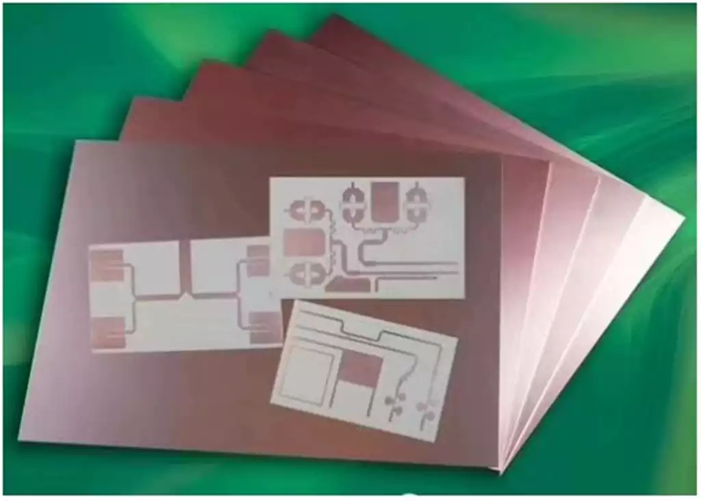
- Insulating substrate:The circuit board uses a non-conductive material as a substrate, such as FR-4 epoxy fiberglass, polytetrafluoroethylene (PTFE), polyimide, or ceramic to support and isolate the conductive paths and components in the circuit.
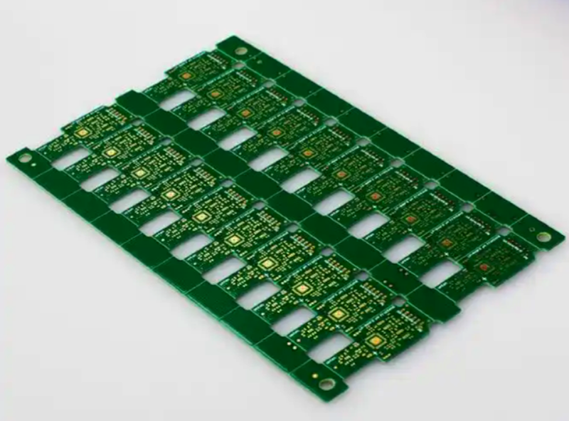
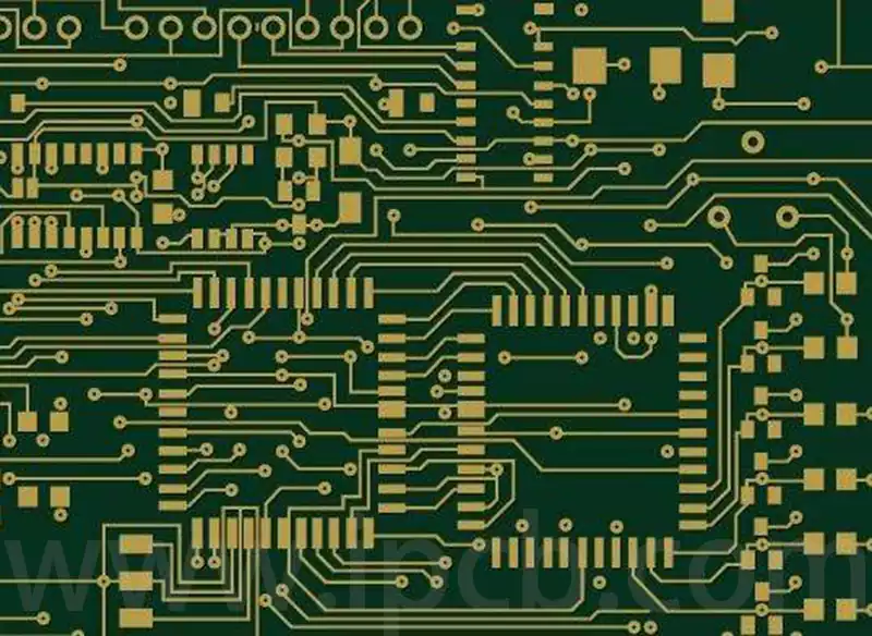
- Conductive Layer:On an insulating substrate, a thin layer of metal, usually copper is formed into a circuit pattern through a chemical etching process. These conductive paths are called traces (traces), they connect the various electronic components, such as resistors, capacitors, transistors, integrated circuits and so on.
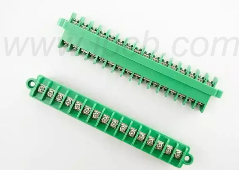
- Component Mounting: Components are mounted in predetermined locations on the circuit board usually by soldering to pads. The pads are metal areas on the circuit board reserved for connection to the pins of the components.

Optimization of the layout of the PCB circuit is a key factor in ensuring the efficient transmission of current. Reasonable layout can enhance the efficiency of current flow, reduce signal interference and power consumption, and improve circuit stability:
When designing circuit boards, components should be laid out so that the current flow path is as short and direct as possible. The shorter the distance between components, the smaller the impedance of current flow, and the delay and interference of signal transformation can be reduced. Therefore, designers should carefully arrange component positions according to circuit function residuals to ensure the efficiency and reliability of signal flow.
Optimizing the signal path is an important step to enhance efficient current transfer. Signal lines should be laid out as short and straight as possible to minimize transmission delays and electromagnetic interference. At the same time, avoid alignment crossings and sharp turns to reduce the possibility of signal reflection and interference. This method is especially suitable for the design of high-speed signal lines.
The design of power and grounding lines is also critical. Wider alignments and shorter paths should be used to reduce inductance and impedance, thus reducing voltage drop and interference. The design can be made with separate ground planes to provide a low impedance path on the one hand and effective noise shielding on the other. A good grounding design helps to improve the stability of the current, thus ensuring a smooth flow of current.
In the circuit, signal fluctuations can be smoothed out by decoupling capacitors to further enhance current transmission. Decoupling capacitors should be placed as close as possible to the pins of the components that require a stable power supply, thus ensuring a stable power supply and fast response. This design can effectively reduce power supply noise and improve circuit performance.
In multilayer circuit boards, the rational use of vias is the key to ensuring current transfer efficiency. The vias should be arranged as close as possible to the power and ground planes to facilitate fast signal switching and efficient connection of routes. Using the method of reducing the number of vias and optimizing their location can avoid the loss of signal transmission between layers, while ensuring the link between layers.
PCB circuit is the core of modern electronic equipment, its design and layout optimization needs to ensure efficient and stable operation of the equipment. With the progress of science and technology, circuit board circuit design continues to innovate to adapt to the complexity of high-speed demand.