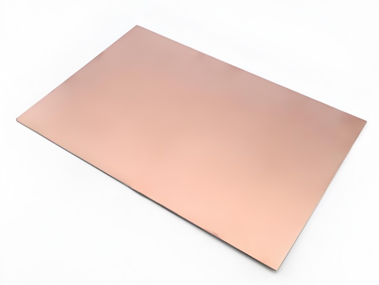
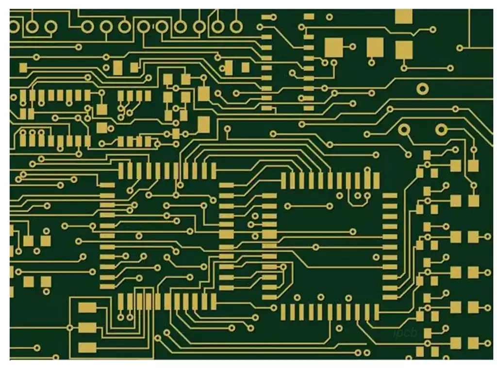
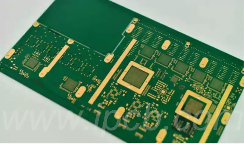
A 3 layer PCB contains three conductive copper layers. The top and bottom outer layers are primarily used for component mounting and signal routing, while the inner layer can be configured as a ground plane, power plane, or additional signal layer according to the specific design requirements.
Compared with a two-layer PCB, a 3 layer PCB provides additional routing space. Compared with a conventional four-layer PCB, it uses fewer copper layers and has a simpler physical structure. However, 3 layer PCBs are not widely used in commercial PCB mass production. The main reason is not inadequate electrical performance, but the significantly greater manufacturing difficulty associated with their asymmetric layer structure. Asymmetric stackups make lamination, copper balancing, warpage control, and stackup design more challenging. In most engineering applications, a four-layer PCB provides a more practical solution for mass production because its symmetrical construction offers better manufacturing stability and more predictable performance.
One of the most commonly used three-layer stackup configurations is Signal/Ground/Signal (S/G/S). In this structure, the top layer is used for component placement and primary signal routing, the middle layer functions as a continuous ground reference plane, and the bottom layer provides additional signal-routing capacity. This configuration provides high-speed signals on the outer layers with a continuous reference plane, which helps improve signal integrity, reduce circuit noise, and support applications with electromagnetic compatibility requirements.
There is currently no universally standardized 3 layer PCB stackup used throughout the industry. The functional assignment of each layer must be determined according to routing density, power distribution architecture, signal transmission speed, impedance-control requirements, PCB thickness, material selection, and the manufacturer’s fabrication capabilities. The stackup should therefore be customized according to the electrical and manufacturing requirements of the specific product.
3 layer PCB Structure and Operating Principle
The physical construction of a 3 layer PCB follows the same fundamental principle as conventional multilayer PCBs. Individual copper layers are separated by dielectric materials, and the complete stackup is consolidated through a high-temperature, high-pressure lamination process. Rigid industrial 3 layer PCBs commonly use FR-4 as the primary insulating substrate, while the electrical function of each conductive layer can be defined according to the circuit architecture.
Conventional 3 layer PCB Layer Configuration
The first layer is generally used for component mounting and primary signal routing.
The second layer can be configured as a ground plane or power distribution plane.
The third layer is typically used for auxiliary signal routing and additional copper areas where appropriate.
When signal integrity is a major design requirement, the middle layer is preferably configured as a continuous ground plane. This arrangement provides a clearly defined return-current path for signals on the outer layers, significantly reduces the signal-loop area, and helps minimize electromagnetic interference. The actual signal-integrity improvement depends on several factors, including dielectric thickness, routing geometry, return-path continuity, and operating frequency.
If the circuit requires dedicated power distribution networks, the middle layer can instead be configured as a power plane to support multiple supply rails. However, this arrangement reduces the available area of the signal reference plane and may weaken the board’s ability to control noise and maintain optimal signal integrity.
Why 3 layer PCBs Are Less Common in Mass Production
The fundamental limitation of a 3 layer PCB is its odd-numbered layer structure, which cannot naturally achieve the same mechanical stress balance as a symmetrical even-layer stackup.
Most mainstream multilayer PCBs use an even number of copper layers, such as four, six, or eight layers. These structures can be designed with a symmetrical stackup around the center of the PCB, which helps balance the mechanical stresses generated during heating, lamination, cooling, and resin flow. This symmetrical construction is highly effective in controlling PCB warpage and twisting during manufacturing.
A 3 layer PCB, by contrast, has an inherently asymmetric structure. If the copper density or copper distribution differs significantly between the two sides of the board, the imbalance in mechanical stress during mass production can easily result in board bending or warpage. The problem becomes more significant for large-format PCBs, heavy-copper constructions, boards with extensive copper areas, and designs with substantial differences in copper density between layers. These products require much tighter control of stackup design and manufacturing processes, placing higher demands on the PCB manufacturer’s process engineering and production capabilities.
Why Four-Layer PCBs Are Usually Preferred
Compared with a 3 layer PCB, a four-layer PCB can achieve a more symmetrical stackup, making mechanical stress balancing easier and providing greater manufacturing stability and process control. A conventional four-layer structure can independently allocate signal, ground, power, and additional signal functions across different layers. This increases routing flexibility, provides a more organized power-distribution structure, and effectively eliminates many of the mechanical stress issues associated with asymmetric stackups.
From a cost perspective, a 3 layer PCB may appear to reduce material consumption because it uses one fewer copper layer. However, this does not necessarily translate into a meaningful reduction in mass-production cost. A 3 layer PCB still requires most of the major multilayer PCB manufacturing processes, including inner-layer imaging and etching, layer registration, drilling, electroless copper deposition, electroplating, lamination, electrical testing, and final inspection. These processes cannot simply be eliminated because the board has one fewer copper layer.
Therefore, reducing a four-layer PCB to a three-layer structure generally does not provide a significant manufacturing cost advantage. Even when the circuit can technically operate with three conductive layers, a four-layer PCB often remains the better engineering choice because it provides greater routing flexibility, more stable mechanical performance, and lower mass-production risk.
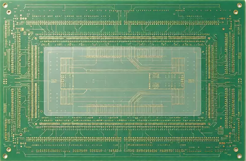
Key Considerations for 3 layer PCB Stackup Design
Stackup design is one of the most important aspects of 3 layer PCB development because it directly affects both electrical performance and manufacturing yield.
For relatively simple circuits, a Signal/Ground/Signal stackup is generally the preferred configuration. A continuous ground plane in the middle layer provides a stable reference for outer-layer traces and, when combined with controlled dielectric thickness, can support controlled-impedance routing. However, simply adding a ground plane does not automatically guarantee good signal integrity. The signal return path must remain continuous and properly defined throughout the entire routing path. High-speed traces must always maintain an appropriate reference-plane relationship, and routing should avoid situations where the return current is forced to cross gaps or discontinuities in the reference plane.
If the middle layer is divided into multiple power domains, the potential impact of signal return currents crossing different power regions must be evaluated in advance. An inappropriate layer-function assignment can interrupt return-current paths and increase electromagnetic coupling and crosstalk. For this reason, the three-layer stackup should be planned together with PCB placement and routing rather than being treated simply as a mechanical layer arrangement. Layer allocation, power distribution, signal routing, and return-current paths should be designed as an integrated electrical system.
Signal Integrity Characteristics of 3 layer PCBs
A 3 layer PCB can support controlled-impedance routing and conventional high-speed circuit designs, but its overall routing flexibility and performance margin are generally lower than those of four-layer and higher-layer-count PCBs.
When the middle layer is configured as a continuous ground plane, outer-layer traces can obtain a stable and predictable return-current path. This helps control trace impedance, reduce the loop area of high-speed signals, and improve transmission performance. Trace impedance is determined by multiple parameters, including trace width, copper thickness, dielectric thickness, dielectric constant, and the distance between the trace and its reference plane. These parameters must be tightly controlled during both PCB design and manufacturing to achieve the required impedance accuracy.
For high-speed interfaces, engineers must also consider the signal-integrity effects associated with via transitions, connector structures, differential-pair routing, reference-plane discontinuities, and other interconnect structures. Because a 3 layer PCB provides fewer reference-plane and routing resources, its suitability for demanding high-speed applications is generally lower than that of a properly optimized four-layer or higher-layer-count PCB.
Key Requirements for Copper Balancing
Copper balancing is one of the most critical considerations in 3 layer PCB design because it plays an important role in reducing mechanical stress imbalance and controlling PCB warpage.
When the copper distribution differs significantly between layers, different areas of the PCB can experience different levels of deformation and stress release during etching, electroplating, thermal cycling, and lamination. These differences can directly contribute to board deformation, warpage, and reduced manufacturing yield.
During PCB layout, the copper distribution across the entire board should therefore be evaluated as a complete system. Without affecting electrical performance, interrupting signal return paths, or creating short-circuit risks, additional copper can be added to otherwise unused areas to improve copper-density balance between layers. Copper balancing does not mean making every layer visually identical. Instead, the copper distribution should be optimized according to copper thickness, dielectric structure, stackup configuration, routing distribution, and the manufacturer’s lamination process.
3 layer PCB Manufacturing Process and Material Selection
Mass-Production Manufacturing Process
3 layer PCBs generally follow the standard multilayer PCB manufacturing process. The process typically includes engineering data preparation and material preparation, inner-layer imaging and etching, inner-layer inspection, dielectric and copper-foil lamination, high-temperature and high-pressure pressing, drilling, hole-wall activation and copper plating, outer-layer circuit fabrication, solder mask application, surface finishing, silkscreen printing, profile machining, electrical testing, and final inspection.
Because 3 layer PCBs still require most of the precision processes used for conventional multilayer boards, their manufacturing complexity is substantially higher than that of standard two-layer PCBs.
Core Material Selection
FR-4 is the most common substrate material for rigid 3 layer PCBs because it provides a balanced combination of electrical insulation, mechanical strength, thermal resistance, manufacturing stability, and cost efficiency.
For specialized applications, alternative substrate materials may be selected according to performance requirements. High-Tg laminates are suitable for applications involving elevated operating temperatures, while high-frequency and low-loss laminates are more appropriate for RF and high-speed circuits. Polyimide materials can be used when a flexible 3 layer PCB structure is required.
Material selection should be based on the electrical, thermal, mechanical, and environmental requirements of the product rather than being determined solely by the number of PCB layers. For controlled-impedance applications, particular attention should be given to the dielectric constant of the laminate and the dielectric thickness between the signal layer and its reference plane to ensure that the manufactured impedance remains within the required tolerance.
Advantages and Limitations of 3 layer PCBs
Key Advantages
Compared with a two-layer PCB, a 3 layer PCB provides an additional internal layer that can be used for signal routing, power distribution, or grounding. This additional routing resource can alleviate routing congestion, support more compact circuit layouts, and facilitate component placement on both sides of the board.
When the middle layer is configured as a continuous ground plane, a 3 layer PCB can also provide improved signal integrity and electromagnetic immunity. This configuration can meet the requirements of many conventional high-speed circuits and precision analog circuits.
The structure is also less complex than that of a conventional four-layer PCB in terms of the number of conductive layers, making it potentially suitable for specialized applications where a full four-layer architecture would provide unnecessary routing capacity.
Major Limitations
The primary limitation is the asymmetric odd-layer structure, which can create mechanical stress imbalance and increase the risk of PCB warpage. The manufacturing process is therefore more difficult to control, and maintaining consistent production yield can be challenging.
3 layer PCBs also provide fewer routing and power-distribution resources than four-layer boards. This limits their suitability for high-density, high-pin-count, high-speed, and high-power circuits.
In addition, the manufacturing process remains broadly comparable to that of conventional multilayer PCBs. As a result, three-layer construction generally cannot provide a significant advantage in either manufacturing cost or production lead time.
Applications of 3 layer PCBs
3 layer PCBs are generally recommended only for applications with specific engineering requirements. They may be considered when a two-layer PCB does not provide sufficient routing capacity, while a four-layer PCB would introduce unnecessary routing resources, and the product architecture, mechanical dimensions, or existing system constraints require an odd-layer structure.
They may also be suitable when a specific routing bottleneck can be completely resolved by adding only one internal layer and the additional routing capacity of a four-layer PCB would not provide meaningful engineering benefits.
When there are no specific structural constraints, a symmetrical four-layer PCB is generally the preferred solution. PCB layer-count selection should be based primarily on electrical performance, manufacturing stability, mechanical compatibility, and overall production risk rather than the assumption that fewer layers will always result in lower cost.
3 layer PCB Compared with Two-Layer and Four-Layer PCBs
3 layer PCB vs Two-Layer PCB
A two-layer PCB contains only the top and bottom copper layers and does not have an internal conductive layer. Its available routing space and options for dedicated ground or power distribution are therefore limited, making it primarily suitable for relatively simple conventional circuits.
A 3 layer PCB adds an internal conductive layer, providing additional routing capacity and allowing a dedicated reference plane or power-distribution layer to be incorporated into the design. This makes it suitable for more complex and higher-precision circuits. However, the additional layer also introduces the manufacturing complexity associated with multilayer PCB fabrication.
3 layer PCB vs Four-Layer PCB
The primary difference between three-layer and four-layer PCBs is not simply the number of copper layers. The more important differences involve stackup symmetry, performance margin, routing resources, and mass-production stability.
A four-layer PCB can use a symmetrical stackup to achieve better mechanical stress balance while providing sufficient routing capacity for independent signal, ground, and power-plane configurations. This produces more predictable return-current paths and generally provides better electromagnetic compatibility and signal-integrity performance. Four-layer PCBs are therefore suitable for a broad range of medium- and high-complexity, high-density, and high-speed electronic products.
3 layer PCBs, by comparison, are better regarded as specialized solutions for specific engineering requirements rather than as a general replacement for conventional multilayer PCB architectures.
General Design Guidelines for 3 layer PCBs
The functional assignment of each PCB layer should be defined at the beginning of the design process. Signal, ground, and power layers should be allocated according to the circuit architecture, and the expected signal return paths should be established before detailed routing begins.
The copper distribution across the entire PCB should be evaluated and balanced during layout. Large areas of copper and significant differences in copper density between layers should be carefully controlled to reduce the risk of mechanical stress imbalance and PCB warpage.
High-speed traces should maintain a continuous reference plane throughout their entire routing path. Differential pairs should follow the specified impedance, spacing, and routing requirements, while via transitions and other discontinuities should be carefully controlled to minimize signal-integrity degradation.
For high-precision or high-complexity PCBs involving controlled impedance, fine-line routing, heavy copper, large board dimensions, or other demanding manufacturing requirements, the proposed stackup and critical fabrication parameters should be reviewed with the PCB manufacturer before production release. This ensures that the electrical design requirements are compatible with the manufacturer’s actual fabrication capabilities.
A 3 layer PCB is a specialized multilayer circuit board positioned between conventional two-layer and four-layer PCB structures. Compared with a two-layer PCB, it provides additional routing capacity and can achieve improved signal integrity when an appropriate internal reference plane is used. This makes it capable of supporting certain medium-complexity and customized circuit designs.
However, its inherent odd-layer and asymmetric structure creates challenges in mechanical stress balancing, copper distribution, lamination, and warpage control. At the same time, its manufacturing process remains largely comparable to that of conventional multilayer PCBs, which means that the reduction of one copper layer does not necessarily produce a meaningful cost or lead-time advantage.
For these reasons, 3 layer PCBs remain a relatively niche solution in commercial PCB mass production. Unless a specific mechanical, electrical, or architectural requirement makes a three-layer structure necessary, a symmetrical four-layer PCB is generally the more practical choice because it provides greater routing flexibility, better mechanical stability, more predictable manufacturing performance, and lower production risk.