As the most widely used entry-level multilayer PCB, the 4 layer PCB provides an ideal balance between electrical performance, routing flexibility, manufacturing complexity, and production cost. Today, it is extensively used in consumer electronics, industrial automation, communication equipment, and numerous other electronic applications.
Core Structure of a 4 Layer PCB
Base Material
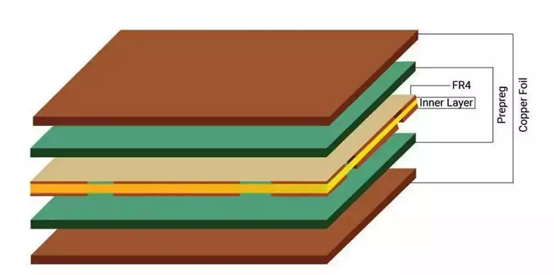
The substrate of a 4 layer PCB is typically manufactured from FR-4 glass fiber-reinforced epoxy laminate, which offers excellent mechanical strength, dimensional stability, electrical insulation, and impact resistance. This material withstands moderate mechanical stress, bending, and vibration during operation while preventing electrical leakage between conductive layers. As the structural foundation of the PCB, it ensures board flatness, mechanical reliability, and long-term durability.
Copper Circuit Layers
The conductive layers are fabricated using high-purity electrolytic copper foil. Through precision manufacturing processes such as photolithography, exposure, development, and chemical etching, the copper foil is patterned into signal traces, solder pads, power networks, and other conductive features.
As the primary medium for power distribution and signal transmission, the quality of the copper foil and the precision of circuit patterning directly determine the PCB’s electrical performance, current-carrying capability, and signal transmission efficiency.
Dielectric Insulation Layers
Dielectric materials are laminated between adjacent copper layers to provide complete electrical insulation throughout the multilayer structure. Their primary function is to prevent electrical short circuits between conductive layers while maintaining precise layer spacing.
In addition to electrical isolation, the dielectric layers bond tightly with the substrate, enhancing the overall mechanical rigidity of the PCB board and maintaining dimensional stability throughout repeated thermal cycles.
Solder Mask Layer
The outer surfaces of the PCB board are coated with a solder mask, which serves as the primary protective layer for exposed copper circuitry.
Besides preventing copper oxidation and corrosion, the solder mask eliminates solder bridging during assembly while protecting the circuit board from moisture, dust, chemical contamination, and minor mechanical abrasion. As a result, it significantly improves both manufacturing reliability and the service life of the PCB board.
Functions of Each Layer in a 4 layer PCB
Top Layer
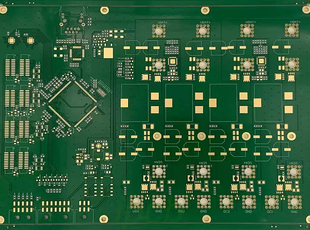
The Top Layer is the outermost signal layer and serves as the primary area for component mounting and signal routing.
Surface-mounted and through-hole components are assembled on this layer, while critical signal traces are routed to establish the primary electrical connections. Test points are also commonly incorporated to facilitate in-circuit testing (ICT), debugging, and maintenance during manufacturing and after deployment.
Bottom Layer
The Bottom Layer forms the opposite outer surface of the PCB board and interfaces directly with the mechanical enclosure or mounting structure.
Besides accommodating additional components and signal routing, this layer is frequently used for extensive ground copper pours and grounding networks that improve electrical performance while optimizing routing density.
Internal Signal Layer
The Internal Signal Layer is located between the power and ground planes and primarily carries high-density signal routing for complex circuits.
By utilizing blind vias, buried vias, and plated through holes (PTH), this layer establishes electrical connections with both outer layers while supporting routing topologies that cannot be achieved with single sided or double sided PCBs.
The symmetrical multilayer structure also helps distribute internal mechanical stress evenly, minimizing board warpage during fabrication and assembly.
Internal Power and Ground Layers
Dedicated Power Plane and Ground Plane layers form the electrical backbone of a 4 layer PCB.
These continuous copper planes distribute stable power throughout the circuit while providing a low-impedance return path for signal currents. More importantly, they play a critical role in electromagnetic compatibility (EMC) design by reducing electromagnetic interference (EMI), suppressing crosstalk, and minimizing electromagnetic radiation.
Compared with double-layer PCBs that rely on fragmented ground routing, the dedicated power and ground planes of a 4 layer PCB offer substantially better electrical performance and signal stability.
Key Advantages of 4 layer PCB Stack-Up Design
Improved Signal Integrity
A properly designed 4 layer pcb stack-up significantly enhances signal integrity.
The closely coupled power and ground planes form an effective distributed plane capacitor, providing excellent power decoupling and suppressing power supply noise. At the same time, the continuous ground plane creates a low-inductance return path that minimizes signal reflection, insertion loss, waveform distortion, and timing errors, ensuring stable transmission of high-speed digital signals.
Enhanced Electromagnetic Compatibility
The internal copper planes naturally provide effective electromagnetic shielding.
The combination of dedicated power and ground layers forms an enclosed shielding structure that both suppresses electromagnetic emissions generated by the PCB and protects sensitive circuits from external electromagnetic interference.
Proper stack-up design also minimizes electromagnetic coupling between adjacent traces, significantly reducing crosstalk and ensuring compliance with EMC regulations.
Greater Routing Flexibility
Compared with conventional two-layer PCBs, a 4 layer PCB adopts a dual outer-layer plus dual inner-layer architecture that dramatically increases available routing resources.
High-speed and critical signal traces can be placed on the outer layers, while the inner layers accommodate power distribution, ground planes, and sensitive signal routing. This arrangement greatly reduces routing congestion and allows designers to implement far more complex circuit layouts within the same board area.
As a result, 4 layer PCBs support higher component density and greater functional integration while simplifying routing optimization.
Superior Mechanical Reliability
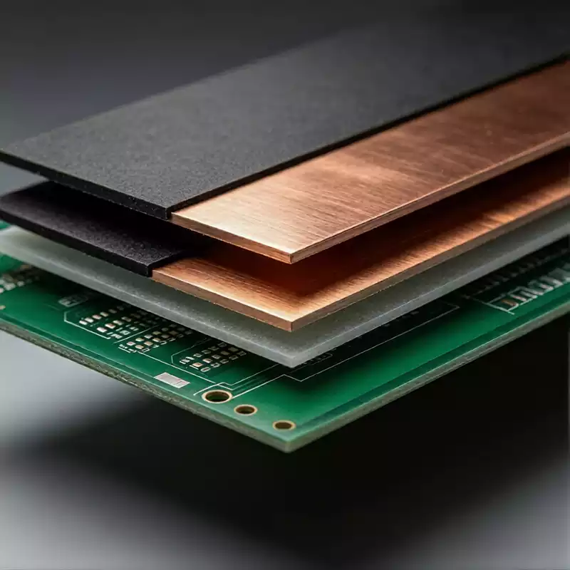
The multilayer laminated construction substantially improves the mechanical strength and rigidity of the PCB board.
The bonding prepreg securely laminates the conductive and dielectric layers into a unified structure capable of resisting vibration, mechanical shock, thermal expansion, and external stress.
Compared with single-layer and double-layer PCBs, 4 layer pcbs exhibit significantly better resistance to warpage, cracking, and delamination, making them particularly suitable for industrial control systems, communication equipment, and other demanding operating environments.
Applications of 4 layer PCBs
In consumer electronics, 4 layer PCBs are widely used in smart home devices, portable multimedia products, wearable electronics, and numerous other compact electronic products. These devices typically integrate multiple functional modules while maintaining strict manufacturing cost targets. The routing capacity and cost efficiency of 4 layer PCBs make them an ideal solution for mass production.
In industrial automation, 4 layer PCBs are commonly found in industrial control boards, sensor interface modules, programmable controllers, and automation equipment. Their multilayer architecture enables physical separation of analog and digital circuits, reducing interference while providing sufficient routing resources for protection circuits, communication interfaces, and system expansion.
In communication equipment, 4 layer PCBs are extensively used in data communication modules, RF front-end circuits, network interface boards, and signal transmission units. Their excellent EMC performance and superior signal isolation ensure reliable high-frequency signal transmission while maintaining competitive manufacturing costs for high-volume production.
As electronic products continue to evolve toward miniaturization, higher operating frequencies, faster data transmission, greater precision, and environmentally sustainable manufacturing, 4 layer PCB materials, fabrication technologies, and design methodologies are undergoing continuous innovation.