Characteristic impedance is one of the most critical parameters in high-speed PCB design. It refers to the dynamic opposition encountered by high-frequency electrical signals as they propagate through PCB transmission lines in the form of electromagnetic waves. Fundamentally, characteristic impedance is defined as the ratio of the instantaneous voltage to the instantaneous current along a transmission line. It is fundamentally different from conventional DC resistance, and the two concepts should never be confused.
DC resistance only describes the opposition of a conductor to steady direct current and depends solely on the conductor’s material, cross-sectional area, and length. Characteristic impedance, by contrast, is a transmission-line parameter that only applies to high-frequency alternating signals. Once signal frequencies enter the high-speed domain, PCB traces no longer behave as simple conductors—they become transmission lines with electromagnetic propagation characteristics. Signals travel as electromagnetic waves through the coupled structure formed by the copper trace and the PCB dielectric. Consequently, the characteristic impedance is determined by multiple factors, including trace geometry, dielectric properties, copper characteristics, and stack-up configuration, making it a comprehensive electromagnetic transmission parameter rather than a simple resistive value.
The primary objective of impedance matching is to eliminate signal loss, reflections, and waveform distortion during transmission, ensuring accurate point-to-point signal delivery. It is one of the fundamental requirements for maintaining signal integrity in high-speed electronic circuits.
Engineering Guidelines for High-Speed PCB Impedance Matching
1.Design with manufacturing capability in mind and allow for process tolerances
Impedance control should not be based solely on theoretical calculations. Manufacturing tolerances—including trace width variation, copper thickness tolerance, dielectric thickness variation, and etching compensation—must be incorporated into impedance simulations during the design stage. IPCB provides free pre-layout impedance simulation services, generating accurate stack-up and impedance reports based on customers’ design files and production capabilities to minimize manufacturing risks before fabrication begins.
2.Select high-quality PCB materials to establish a stable impedance foundation
The stability of the dielectric constant (Dk), copper thickness uniformity, and substrate flatness directly determine the achievable impedance accuracy. Material selection should match the application requirements. Standard high-speed digital applications typically use high-quality Tg130–Tg170 FR-4 laminates from manufacturers such as Kingboard and Shengyi, while high-frequency and ultra-high-speed designs are better suited to specialized RF laminates from Rogers or Taiwan Union Technology (TUC). Halogen-free, black-core, and white-core materials are also available to meet specialized application requirements.
3.Account for the influence of the solder mask
For surface microstrip transmission lines, the solder mask coating typically changes the characteristic impedance by approximately 3% to 8%. Therefore, solder mask thickness and dielectric properties must be included in impedance simulations to prevent discrepancies between calculated and measured impedance values.
4.Route high-speed differential signals on inner layers whenever possible
Stripline routing within internal PCB layers provides reference planes above and below the signal trace, offering superior electromagnetic shielding and more stable impedance while significantly reducing EMI. If routing on an outer layer is unavoidable, ensure that the reference plane beneath the trace remains continuous without splits, voids, or interruptions to prevent impedance discontinuities.
5.Place ground return vias adjacent to signal vias
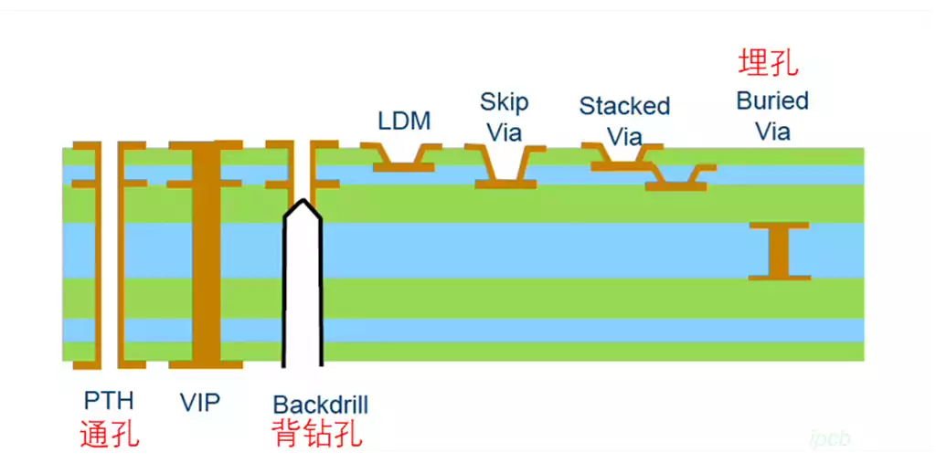
Whenever a high-speed signal transitions between PCB layers through a via, matched ground return vias should be placed as close as possible to the signal via. This provides a continuous return current path, minimizing impedance discontinuities, signal reflections, and return path discontinuities caused by layer transitions.
6.Reserve sufficient routing space and maintain consistent routing geometry
Adequate routing space for differential pairs should be planned during PCB layout to avoid compromising trace spacing during later routing stages. Differential traces should use 45-degree bends or smooth arcs instead of right-angle corners, while maintaining consistent trace width and spacing throughout the entire routing path to eliminate localized impedance variations and preserve signal integrity.
Six Key Factors That Affect Characteristic Impedance
Characteristic impedance is influenced by multiple electrical and physical parameters of the PCB. Among them, the following six factors have the greatest impact:
Dielectric Thickness (H) – The Most Influential Factor
Dielectric thickness refers to the vertical distance between the signal trace and its reference plane. As the dielectric thickness increases, the electromagnetic field extends over a longer propagation path, resulting in a higher characteristic impedance. Variations in dielectric thickness are therefore the primary source of impedance deviation.
Dielectric Constant (Dk) – The Second Most Important Factor
The dielectric constant is an intrinsic property of the PCB laminate. A higher dielectric constant provides stronger electromagnetic field confinement, reducing the characteristic impedance while also affecting signal propagation velocity. Maintaining a stable Dk is essential for achieving consistent impedance control.
Trace Width (W) – The Third Most Influential Factor
Trace width defines the conductor width of the signal line. Increasing the trace width enlarges the current-carrying cross-sectional area and reduces electromagnetic field concentration, thereby lowering the characteristic impedance. Since trace width can be easily adjusted during PCB layout, it is the most commonly optimized design parameter for impedance control.
Copper Thickness (T) – The Least Influential Parameter
Copper thickness refers to the thickness of the PCB copper foil. Thicker copper reduces conductor resistance and slightly lowers the characteristic impedance. However, compared with dielectric thickness, dielectric constant, and trace width, its overall influence on impedance is relatively small.
Differential Pair Spacing (S)
Differential pair spacing is the distance between the two traces of a differential signal pair. Increasing the spacing weakens electromagnetic coupling between the traces, resulting in higher differential and single-ended impedance values. Proper spacing is essential for achieving the target differential impedance.
Transmission Line Structure
The transmission line configuration—including microstrip, stripline, and coplanar waveguide (CPW)—has a significant impact on characteristic impedance. Even with identical material properties and trace dimensions, different transmission line structures produce substantially different impedance values, making transmission line selection one of the most important considerations during PCB stack-up design.
Characteristic Impedance Calculation Models for High-Speed PCB Routing
Accurate impedance calculation depends on selecting the appropriate transmission line model. In PCB design, microstrip and stripline are the two most widely used transmission line structures, each with distinct applications and calculation methods.
A microstrip is located on an outer PCB layer, with the signal trace positioned above a dielectric layer and a reference plane, while the top surface is exposed to air or covered by a solder mask. Its simple structure and routing flexibility make it the preferred choice for many high-speed surface-layer signals. However, the dielectric properties and thickness of the solder mask typically change the characteristic impedance by approximately 3% to 8%. Therefore, solder mask effects must be included in impedance simulations to prevent discrepancies between calculated and measured values.
A stripline is routed within the internal layers of a PCB and is completely enclosed between two reference planes. This symmetrical structure provides superior electromagnetic shielding, lower EMI, and more stable impedance characteristics, making stripline the preferred transmission line for high-speed, high-precision signal routing.
In practical engineering, characteristic impedance is rarely calculated manually using analytical equations. Instead, designers rely on professional field-solver software. Industry-standard tools such as the Polar Si9000 Impedance Calculator and the impedance calculation modules integrated into EDA software such as Altium Designer allow engineers to enter parameters including dielectric constant (Dk), copper thickness, dielectric thickness, stack-up configuration, and transmission line structure. The software then accurately calculates the required trace width and spacing to achieve the target impedance while simultaneously simulating the effects of manufacturing tolerances, enabling designers to build appropriate design margins into the PCB.
Why 50 Ω and 100 Ω Have Become Industry Standards
The commonly specified 50 Ω single-ended impedance and 100 Ω differential impedance used in high-speed PCB design are not arbitrary values. Instead, they represent the optimal engineering compromise established through decades of practical experience, balancing signal integrity, power handling capability, and manufacturing feasibility.
The 50 Ω single-ended impedance standard originated from research on RF coaxial cables. Experimental results showed that a 30 Ω transmission line offers maximum power-handling capability but suffers from relatively high signal attenuation and poor transmission stability. In contrast, a 77 Ω transmission line provides the lowest signal loss and highest transmission accuracy but has limited power-handling capability. 50 Ω represents the best compromise between these competing characteristics, making it the universal standard for RF systems and high-speed digital circuits.
Differential impedance standards vary according to interface specifications. 90 Ω differential impedance is specified for the USB family of high-speed interfaces. 100 Ω differential impedance is widely used for HDMI, LVDS, Ethernet, and conventional PCI Express differential channels. 85 Ω differential impedance is commonly specified for PCI Express Gen3 and later high-speed standards.
From a theoretical perspective, a differential pair consisting of two 50 Ω single-ended traces would appear to produce 100 Ω differential impedance. However, because electromagnetic coupling exists between the two conductors, the actual differential impedance deviates from the simple sum of the individual impedances. Therefore, accurate differential impedance must always be calculated using a 2D electromagnetic field solver rather than by simple arithmetic estimation.
Tight Control of Trace Width to Minimize Impedance Variation
Trace width is the most sensitive adjustable parameter affecting characteristic impedance. Engineering measurements show that a 1 μm deviation in trace width can cause an impedance variation of approximately 0.8 Ω in the opposite direction. Even extremely small dimensional deviations can therefore result in significant impedance shifts. Consequently, the precision of circuit pattern transfer and copper etching directly determines the achievable accuracy of impedance control.
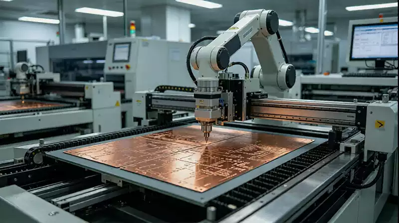
IPCB utilizes a fully automated dry-film lamination process combined with Laser Direct Imaging (LDI) technology, eliminating the inherent limitations of conventional phototool exposure. Without the need for traditional artwork films, LDI enables highly accurate circuit pattern transfer with registration accuracy of ±10 μm and a minimum trace resolution of 40 μm. This advanced process effectively eliminates pattern distortion, layer misalignment, opens, and shorts, ensuring excellent trace width consistency from the beginning of the manufacturing process.
For the etching process, IPCB employs an integrated vacuum precision etching line that combines developing, etching, and resist stripping into a single automated process. A synchronized spray-and-vacuum extraction system continuously removes saturated etchant from the copper surface and replaces it with fresh chemical solution, effectively eliminating the conventional “beach effect” associated with traditional etching processes. This significantly reduces lateral undercutting, improves the etching factor, and maintains uniform trace widths for both heavy-copper and fine-line circuits, resulting in more stable impedance performance across the finished PCB.
Precise Lamination Control Ensures Uniform Dielectric Thickness
Because dielectric thickness is the single most influential factor affecting characteristic impedance, its uniformity is critical for accurate impedance control. The final dielectric thickness is determined during the lamination process and is influenced by prepreg (PP) resin flow, lamination pressure, and temperature uniformity.
IPCB uses high-precision temperature-controlled lamination equipment, maintaining lamination temperature within ±2°C and pressure variation below 5%. The process also incorporates a two-stage lamination cycle consisting of vacuum pre-press degassing followed by final curing, which completely eliminates trapped air between layers while ensuring intimate bonding throughout the PCB stack-up. As a result, dielectric thickness can be controlled within ±5%, providing the process stability required for high-precision impedance-controlled PCB manufacturing.
PCB characteristic impedance control is a comprehensive engineering discipline that spans circuit design, material selection, PCB fabrication, and finished-product verification. It cannot be achieved through theoretical calculations alone. The final impedance of a PCB transmission line is determined by the combined effects of dielectric material properties, transmission line geometry, PCB stack-up, and manufacturing precision. The ultimate goal of impedance matching is to eliminate signal reflections, minimize waveform distortion, and preserve signal integrity, ensuring reliable high-speed signal transmission throughout the entire electronic system.