In the maintenance and repair of high-frequency, microwave, and millimeter-wave circuit boards (such as 5G/6G millimeter-wave antennas, phased-array radars, satellite communication front-ends, and automotive-grade 77GHz radars), “repair” is far more than simply reconnecting wires or replacing components. At frequencies of tens of gigahertz, every micrometer of the physical topology on the PCB directly participates in the guidance and energy conversion of electromagnetic waves. How to fix a circuit board For RF and Microwave PCB?Traditional methods like extensive wiring, large-area soldering, or ordinary epoxy resin filling can lead to severe impedance abrupt changes in microwave transmission lines, surface electromagnetic wave scattering, a dramatic increase in high-frequency dielectric loss, and phase distortion between phased-array channels, causing complete failure of the board’s high-frequency performance.
The repair of high-frequency RF PCBs must be based on rigorous electromagnetic theory, materials physics, and microfabrication engineering. This guide provides an in-depth analysis of the physical damage mechanisms of high-frequency RF PCBs, micrometer-level physical reconstruction processes, BGA/QFP rework fixture control, and the restoration and testing of electromagnetic performance after repair.
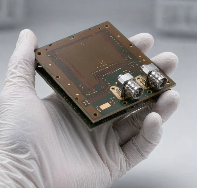
Physical Damage Mechanisms and Electromagnetic Failure Physics of High-Frequency RF Circuit Boards
High-frequency RF circuit boards typically employ special ultra-low loss substrates (such as polytetrafluoroethylene (PTFE) and hydrocarbon ceramic RO4000 series) and ultra-low roughness copper foil (HVLP). Physical damage not only disrupts mechanical integrity but also damages the electromagnetic field distribution at the microscopic level.
The Destructive Effects of Physical Deformation on S-Parameters of Microstrip Lines and Coplanar Waveguides (GCPWs) The characteristic impedance of RF transmission lines (microstrip lines, striplines, GCPWs) is determined by the conductor width, copper foil thickness, dielectric layer thickness, and dielectric constant. When traces undergo micron-level deformation due to impact, scratches, or overcurrent ablation: impedance abrupt changes and reflection loss (S11/S22 deterioration): Even minor changes in trace width or edge burrs can disrupt the balance between distributed capacitance and distributed inductance, causing impedance to deviate from the standard 50Ω. This leads to severe reflection of high-frequency energy at the abrupt change point, forming standing waves, reducing power transmission efficiency, and even breaking down the front-end power amplifier (PA). Radiation Loss and Phase Distortion (S21 Deterioration): Missing copper foil edges or uneven repair surfaces disrupt the confinement of the electromagnetic field, causing quasi-TEM mode electromagnetic waves that originally propagated along the medium to become stray waves radiating into space. In phased array antennas, this deformation also introduces additional group delay, disrupting phase consistency between channels.
Substrate Overheating and Carbonization and Dielectric Physical Degradation: Breakdown or high-frequency arcing in high-frequency high-power devices (such as gallium nitride GaN power amplifiers) can lead to substrate overheating. Conductivity Effect of Carbonized Resin: Organic polymers in the substrate undergo dehydrogenation and carbonization at high temperatures, generating carbon elements with high conductivity, causing the original insulating medium to become a low-impedance path. Dramatic Increase in Dielectric Loss Tangent (Df): Even if the substrate is not completely blackened, microscopic thermal decomposition can destroy the molecular chains of inorganic fillers and resins, causing the Df value to increase by several orders of magnitude. High-frequency electromagnetic waves passing through this region will be converted into severe heat dissipation.
In frequency bands above 10 GHz, the skin effect layer and surface plating damage typically result in a current skin depth of less than 1 micrometer. If, during repair, ordinary immersion nickel gold (ENIG) rich in ferromagnetic nickel or an uneven layer of ordinary solder is used to cover the microstrip line surface, the high-frequency current will be forcibly confined to the high-resistivity or ferromagnetically losing metal layer, leading to an exponential increase in high-frequency conductor losses.
High-frequency non-destructive fault location and microscopic detection technology
For latent faults in high-frequency PCBs (such as broken inner layer striplines, via cracks, or minor physical damage), conventional multimeter DC continuity tests are completely ineffective; high-frequency electromagnetic physical detection methods are necessary.
Time Domain Reflectometer (TDR) for Micrometer-Level Breakpoint Location: TDR injects an extremely steep step pulse into the transmission line and measures the amplitude and time delay of the electromagnetic waves reflected along the line in real time. Based on the polarity and amplitude of the reflected pulse, the physical properties of the damage point can be accurately determined: a positive reflected pulse corresponds to an open circuit or increased impedance (thinner trace, breakage); a negative reflected pulse corresponds to a short circuit or decreased impedance (wider trace, excessive parasitic capacitance). Combined with the propagation speed of electromagnetic waves in a specific medium, TDR can pinpoint the fault location to a physical distance of millimeters or even sub-millimeters.
X-Ray 3D Tomography and Microfocus CT: For inner layer striplines, buried vias, and blind vias in multilayer high-frequency hybrid stack-up boards, the microfocus X-Ray inspection system can non-destructively observe microscopic cracks in the walls of plated vias (PTH), peeling at the bottom of blind vias, and fractures in the inner copper foil.
Micron-level RF transmission line physical reconstruction and flying wire compensation process
The repair of high-frequency traces must not use ordinary thick copper wire or large-area solder buildup. Micron-level precision physical reconstruction technology must be used to ensure a high degree of matching between the geometry and electromagnetic characteristics of the repair area.
Minimally invasive removal and dielectric filling of damaged carbonized substrate: Under a microscope, using a diamond grinding head or micro-engraving tool, all carbonized, discolored substrate and damaged copper foil are thoroughly removed. The edges must be ground into a gradual transition groove with a bevel angle of 30°~45° to avoid electromagnetic stress concentration caused by vertical steps. Low-loss high-frequency resin filling: Ordinary general-purpose epoxy resin is strictly prohibited. High-frequency specialized filler resin or ceramic-free glass microsphere filler adhesive must be used, with dielectric constant and dielectric loss (Dk/Df) highly matched to the original substrate (such as RO4350B or PTFE). Curing and precision leveling: After heat curing, a micro-polishing machine is used to grind and polish the filled area until it is absolutely flush with the original substrate dielectric layer, with a surface roughness Ra less than 0.4 micrometers.
Microstrip line and coplanar waveguide (GCPW) copper foil reconstruction: For broken or missing microstrip lines, ultra-thin copper foil patch micro-soldering technology or high-frequency specialized coplanar microstrip bridging technology are mainly used. Material Selection: Use ultra-low roughness rolled copper foil (HVLP, typically 18 µm or 35 µm thick), identical to the original board.
Geometric Topology Alignment: Use a micro-dicing tool to cut the copper foil for soldering into a rectangle perfectly matching the width of the original trace. Any outward-extending burrs or sharp corners are strictly prohibited (sharp corners will generate severe end effects and tip discharge at high frequencies).
Overlap and Micro-Soldering: Place the copper foil for soldering at the break point, maintaining a minimal overlap of 0.2~0.5 mm between both ends and the original trace. Use a high-precision pulsed laser soldering machine or a micro parallel seam soldering machine for spot welding, avoiding thick solder buildup.
Taper Compensation: If a slight increase in thickness is unavoidable at the overlap, the overlap edge must be ground into a very small, gradual slope structure to smoothly transition the excessively small parasitic inductance.
Physical reconstruction of via fencing in the repair of coplanar waveguides (GCPWs) or shielded areas: Damage to the via fencing on both sides can lead to severe electromagnetic leakage. Via fencing physical puncture: Re-drill the via using a micro-drill bit on the repaired medium. Copper sleeve insertion and double-sided soldering: Insert micro-plated copper hollow needles or pure copper conductive needles, and solder both ends flush with the top and bottom layer grounding copper foils respectively. Spacing control: Strictly ensure that the center-to-center spacing of the reconstructed vias is less than one-tenth of the wavelength of the highest operating frequency in the medium.
High-frequency BGA/QFP chip-level rework and soldering
Rework of metallurgical control RF chips (such as MMICs, RF transceivers, high-frequency PAs) not only requires non-destructive desoldering but also places extreme demands on the micro-metallurgical structure and parasitic parameter control of the solder joints.
Rework temperature profile and thermal stress control: High-frequency substrates (especially PTFE substrates) have a large coefficient of thermal expansion (CTE) in the Z-axis direction. Rapid heating can easily lead to breakage of inner layer vias or blistering and peeling of the substrate. Bottom preheating: Use a large-area infrared preheating stage to uniformly preheat the entire board to 100℃~120℃ to reduce local thermal stress. Dedicated RF rework nozzle: Use a hot air desoldering station with an airflow dispersion mesh, strictly following the preset four-stage heating curve of “preheating – heat preservation – reflow – cooling,” controlling the peak temperature at 240℃~250℃ (lead-free process), with a duration not exceeding 30 seconds.
Pad flatness and IMC (intermetallic compound) thickness control: Solder wicking and cleaning: After chip removal, use braided solder wicking tape with a flat-head soldering iron to clean the pads. The residual solder height difference must be controlled within ±5 micrometers; otherwise, BGA resoldering will cause chip tilting, altering the distributed capacitance of high-frequency pins. Eutectic Solder Joint Control: Controlling the eutectic time during soldering avoids the formation of excessively thick non-conductive or high-impedance intermetallic compounds (IMC layers that are too thick can lead to thermal fatigue cracking at high frequencies and high power).
Fluoride Residue and High-Frequency Cleaning Flux Residue: Flux residue is an insulator at low frequencies, but at frequencies above several GHz, it exhibits significant dielectric loss and hygroscopicity, leading to extremely high high-frequency surface attenuation. Ultrasonic/Spray Cleaning: After rework, high-purity isopropanol (IPA) or a dedicated RF cleaner must be used, along with a stereomicroscope, to thoroughly remove all flux residue under chip pins and in microstrip line gaps.
Inner Layer Stripline and Buried/Blind Via Physical Reconstruction Technology
Repairing inner layer signal damage on multilayer high-frequency hybrid boards (such as Rogers + FR-4 6-layer/8-layer boards) is the pinnacle challenge in PCB rework.
Deep controlled step-peeling exposes damaged strips of inner layers. It requires laser milling or high-precision controlled-depth milling cutters to peel away the dielectric layer and copper foil above the damaged area layer by layer in a step-like manner, creating an exposed internal physical working surface.
Controlled-depth backdrilling for stub removal and micro-via repair: When a cross-layer via is damaged, if unused via segments (stubs) remain, at high frequencies, these stubs will act as quarter-wavelength notch filters, causing complete signal interruption in specific frequency bands.
Precision backdrilling: Using a micro-drill bit 0.1mm larger than the original hole diameter, the damaged via and residual stubs are completely removed.
Conductive micro-filling: Micro-conductive copper rods are inserted, connecting only the designated signal layers. Non-connecting layers are isolated with insulating resin, reconstructing a high-frequency via channel without residual stubs.
Electrical Performance Restoration and Conformal Coating
After completing the physical microstructure, the repaired area must undergo electromagnetic coating protection and rigorous RF performance verification.
Recessed Solder Mask and Moisture-Proof Coating: Ordinary green solder mask layers have extremely high dielectric loss. Direct coverage with ordinary solder mask ink is strictly prohibited in the microstrip backbone region above 6 GHz.
Solder Mask Defined: The microstrip line surface in the repaired area should remain bare or covered only with a low-loss, low-dielectric-constant organic conformal coating (such as a poly(dimethyl terephthalate) coating).
Edge Sealing: Apply a small amount of UV-cured high-frequency solder mask only at the dielectric repair joint to prevent moisture from penetrating the molecular gaps in the high-frequency substrate.
RF Performance Network Analyzer (VNA) Verification Testing
Before formal delivery, the repaired circuit board must undergo S-parameter scan testing using a Vector Network Analyzer (VNA):
Reflection Coefficient (S11/S22) Test: Within the operating frequency band (e.g., 24GHz-28GHz), the repaired port VSWR should be less than 1.5 (reflection loss S11 less than -14 dB), confirming no severe impedance discontinuities.
Transmission Coefficient (S21) and Insertion Loss Test: Compared to standard undamaged traces, the increment of insertion loss after repair should be controlled within a stringent range of less than 0.2 dB to 0.5 dB within the target frequency band.
Phase and Group Delay Test: For multi-channel phased or differential high-frequency traces, measure the phase difference between the repaired channel and the adjacent standard channel to ensure the phase deviation meets the system phase compensation margin requirements.