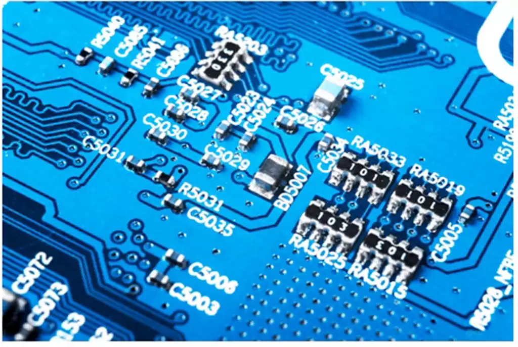
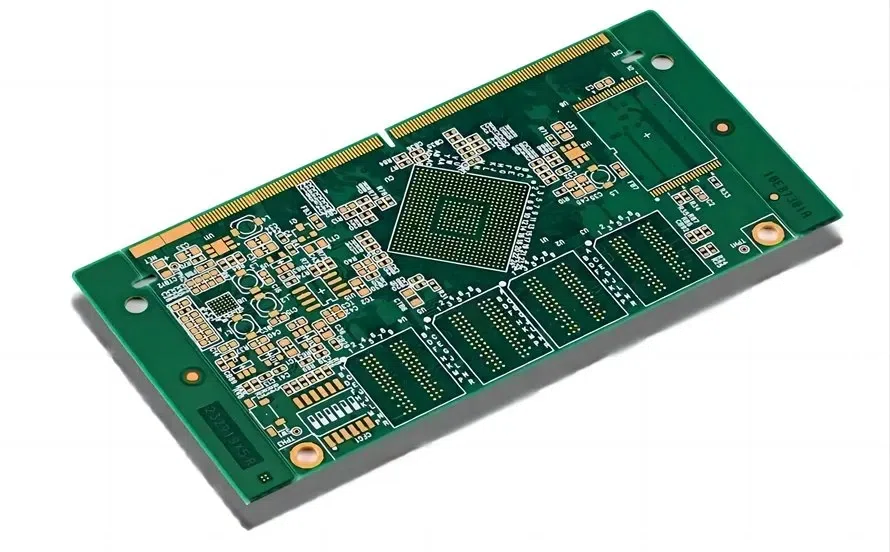
A PCB board is a physical structure fabricated by translating electronic circuit designs into conductive copper traces, dielectric substrates, holes and protective layers. Though a finished PCB appears to be a simple flat panel, its production involves a series of tightly‑controlled manufacturing steps, including computer‑aided manufacturing, copper circuit formation, photolithography, etching, drilling, plating, lamination, solder mask application, surface finishing and electrical testing.
The exact workflow varies with board types: single‑sided PCB, double‑sided PCB, multilayer PCB, rigid PCB, flexible PCB, and boards with advanced features such as microvias and high‑density interconnect (HDI) structures. For conventional multilayer PCBs, fabricators first process bill‑of‑materials and manufacturing outputs derived from PCB designs, then progressively convert copper‑clad laminates into finished circuit boards.
PCB manufacturing commences prior to bare panel loading on the production floor. Engineers develop schematic capture and PCB layout, defining component footprints, copper traces, pads, vias, board dimensions, stack‑up configuration and other design specifications. Once layout completion and design verification are finished, design files shall be converted into manufacturing data interpretable by production equipment. Gerber files describe individual PCB board layers, including copper artwork, solder mask and silkscreen; drill files define hole locations and hole sizes.
Subject to project requirements, fabricators may additionally request stack‑up documentation, fabrication drawings, netlists, impedance constraints and other production specifications. Computer‑Aided Manufacturing (CAM) software is deployed to review and optimize these files, ensuring accurate translation from digital design to physical PCB board hardware.
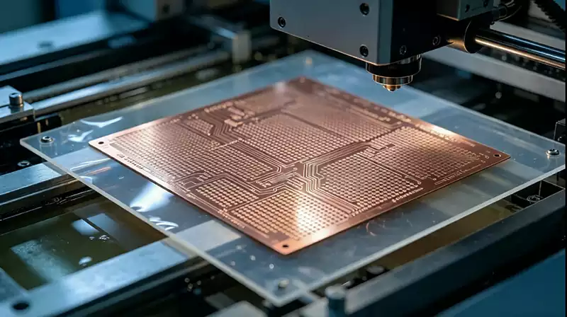
The formation of copper circuitry constitutes the core of PCB fabrication. Standard PCB boards start with dielectric substrates laminated with copper foil; multilayer PCBs adopt a combination of copper‑clad cores and prepreg materials. Target circuit patterns are transferred onto copper surfaces via photolithographic processes. In conventional photolithography, photosensitive dry‑film resist or liquid photoimageable resist is applied over copper foils, followed by exposure per circuit artwork and development. Selected areas are protected by resist masks while other copper regions remain exposed for subsequent processing. Unwanted copper is stripped away by chemical etching, retaining copper traces and pads that establish electrical interconnections. This workflow enables the PCB industry to produce ultra‑fine circuit geometries directly from digital datasets.
Inner‑layer circuits for multilayer PCBs are fabricated separately before being assembled into the final stack‑up. Each inner layer carries dedicated circuit patterns, and precise layer‑to‑layer registration is mandatory; minor registration offset will degrade inter‑layer connectivity. After inner‑layer imaging and etching, copper surfaces undergo surface roughening treatment to enhance lamination adhesion. Circuit layers are interleaved with dielectric prepreg sheets and consolidated under controlled temperature and pressure. During lamination, resin within prepreg flows and cures, bonding discrete layers into an integrated multilayer panel. The Association Connecting Electronics Industries (IPC) identifies inner‑layer fabrication, photolithography, circuit formation, inner‑layer surface treatment, lay‑up and press cycles as critical procedures for multilayer PCB production.
Upon completion of multilayer lamination, panels are drilled in accordance with manufacturing datasets. Holes serve multiple functions: some accommodate component mounting, while others act as vias providing electrical interconnections between different copper layers. Vias are essential for multilayer PCBs, as signal and power nets frequently traverse multiple layers instead of residing on a single plane. Conventional through‑holes penetrate the entire board stack‑up; advanced designs implement blind vias, buried vias or microvias to achieve higher routing density. For holes intended for inter‑layer conduction, drilled hole‑walls must be made conductive by copper electroplating, which deposits metallic copper onto inner hole‑wall surfaces.
Copper plating also participates in outer‑layer circuit build‑up. Depending on production methodologies, panels may implement different combinations of panel plating and pattern plating. According to IPC technical documents, panel plating refers to the process where drilled panels are fully copper‑plated prior to photosensitive etch‑resist lamination, imaging and subsequent etching. Process sequences differ across board constructions and fabrication routes, yet the objective remains consistent: produce dimensionally‑stable copper features with adequate mechanical robustness and electrical integrity.
Following copper feature formation and plating, functional protective coatings are applied onto PCB outer surfaces. Solder mask, the most recognizable colored surface coating, covers most panel areas and exposes designated pads for soldering operations. Solder mask protects copper conductors from environmental corrosion and prevents unintended solder bridging during assembly. Silkscreen marking is implemented where necessary to print reference designators, polarity symbols, part identifiers and other marking information. Silkscreen features normally do not participate in electrical conduction but facilitate assembly, inspection, rework and product traceability.
Exposed copper pads require appropriate surface finish. Surface finishes preserve exposed copper and maintain good solderability. Different surface‑finish selections are determined by component requirements, assembly processes, storage conditions, electrical performance targets and cost budgets. Therefore, surface finish counts as a formal PCB specification rather than purely cosmetic treatment. After surface‑finish completion, bare boards move to final inspection and testing.
PCB quality assurance is not limited to end‑of‑line final inspection. Process‑in‑loop quality control is implemented throughout manufacturing, since defects introduced in upstream operations will compromise downstream processes. Inner‑layer artwork inspection is performed before lamination; layer registration tolerance is monitored during lay‑up and pressing; drilled hole dimensions shall meet drawing requirements; plated structures must guarantee reliable electrical continuity. Final inspection verifies board dimensions, surface condition, solder mask and silkscreen quality, hole characteristics and other acceptance criteria. Electrical test is executed to detect open circuits and short circuits, confirming that the manufactured conductive network matches the original design netlist. PCB industry specifications emphasize that electrical testing and final inspection are indispensable for delivering functional bare PCBs.
Post‑Fabrication of Bare PCB boards
A bare PCB is not a finished electronic product. It delivers only the physical circuit infrastructure; electronic components still need to be mounted and soldered onto pads. This downstream phase is known as PCB assembly, or PCBA manufacturing. Surface‑Mount Technology (SMT) is widely adopted in modern electronics, enabling direct component placement atop PCB surface pads. A typical SMT workflow includes solder‑paste printing via stencil, automated component pick‑and‑place, and conveyor transport through a reflow oven, where solder melts to form robust electrical and mechanical joints. Through‑hole components are inserted through drilled holes and soldered via wave soldering or selective soldering processes. Assembly operations take place subsequent to bare‑board fabrication; hence bare‑PCB manufacturing must be clearly distinguished from PCBA assembly.
PCB Manufacturing Lead Time
PCB lead time is heavily governed by board construction and production requirements. Standard double‑sided PCBs exhibit lower fabrication complexity compared with high‑layer‑count boards featuring fine‑line geometries, controlled impedance, specialty dielectrics, microvias and other advanced structures. Production volume also influences production scheduling: fabricators prepare tooling, raw materials, panelization and production capacity accordingly, so prototyping and high‑volume mass production follow distinct scheduling schemes. Completeness and consistency of manufacturing datasets further affect turnaround time; incomplete or conflicting documentation requires additional engineering review before production release.
Why Multilayer PCB Fabrication Presents Higher Complexity
Manufacturing complexity rises significantly with increased PCB layer count. Double‑sided PCBs only require coordination between top‑side and bottom‑side copper patterns, whereas multilayer PCBs incorporate multiple signal layers, power planes, ground planes, core materials and prepreg sheets. All layers must be designed and manufactured as a complete stack‑up, with inter‑layer positional offsets kept within specified tolerance windows. Fabricators must control drilling and plating processes to ensure vias connect target layers accurately. For high‑speed applications, stack‑up physical properties directly determine electrical performance; dielectric thickness, copper geometry, impedance performance and layer‑to‑layer registration become highly critical parameters.
When all unit processes are integrated, the full PCB manufacturing logic can be summarized as follows: electronic circuit designs generate manufacturing datasets; fabricators validate datasets with CAM software and prepare copper‑clad raw materials; inner‑layer circuits are manufactured and laminated for multilayer constructions; drilling generates component mounting holes and various via structures; copper plating establishes inter‑layer electrical conduction; outer‑layer circuits are formed, followed by solder‑mask and silkscreen application; exposed pads receive specified surface finish; finished panels undergo dimensional, visual and electrical inspection. Upon finishing all steps, bare PCBs are delivered and ready for component assembly.
Process flows vary among different PCB board types, as not all boards share identical materials or technology sets. Simple single‑sided PCBs involve minimal process steps; high‑density multilayer PCBs demand extensive inner‑layer processing, sequential lamination, precision drilling, controlled plating, fine‑line photolithography and comprehensive inspection routines. Flexible PCBs, rigid‑flex PCBs, high‑frequency PCBs, ceramic PCBs and HDI PCBs impose unique material and process constraints. Nevertheless, the underlying principle stays unchanged: PCB manufacturing transforms digital circuit designs into precisely‑patterned physical substrates to deliver reliable interconnections between electronic components.
PCB boards are produced through a sequence of operations including digital engineering, copper circuit formation, photolithography, etching, lamination, drilling, plating, protective coating, surface finishing and inspection. Manufacturing originates from PCB design data instead of pre‑formed physical panels; each process step progressively materializes digital designs into tangible hardware. Copper foils constitute conductive networks; dielectric materials isolate circuit layers; vias realize cross‑layer interconnections; solder mask protects panel surfaces; surface finishes secure pad solderability for subsequent assembly.