For beginners learning about PCBs, one of the most common sources of confusion is the difference between a PCB schematic and a PCB layout file. Although these two files are closely related, they represent two completely independent stages of the PCB development process. Understanding their definitions, functions, and characteristics is essential for successful PCB design, prototyping, and mass production. This article explains the key differences, structural elements, and practical applications of both.
To understand the distinction between these two types of files, it is first important to understand what a PCB is. A Printed Circuit Board (PCB) is the fundamental platform that mechanically supports and electrically connects electronic components in virtually all electronic devices. The familiar green circuit board found in most electronic products is the most common example of a PCB.
The PCB schematic and the PCB layout file represent two major stages of PCB development. Their primary difference is that a schematic focuses on the circuit’s electrical logic, while the layout file defines the board’s physical implementation. PCB development always follows a fixed workflow: the schematic is created first, followed by the PCB layout.
A PCB schematic is the starting point of every circuit board design project and serves as the engineering blueprint of the circuit. It uses standardized electronic symbols to illustrate all electronic components, their electrical characteristics, and the logical electrical connections between them in a two-dimensional diagram.
It is important to understand that a schematic defines only the electrical connectivity and functional behavior of the circuit. It does not specify the physical locations of components, PCB routing, or the actual mechanical arrangement of the board. Instead, it enables engineers to quickly understand how the entire circuit operates from an electrical perspective.
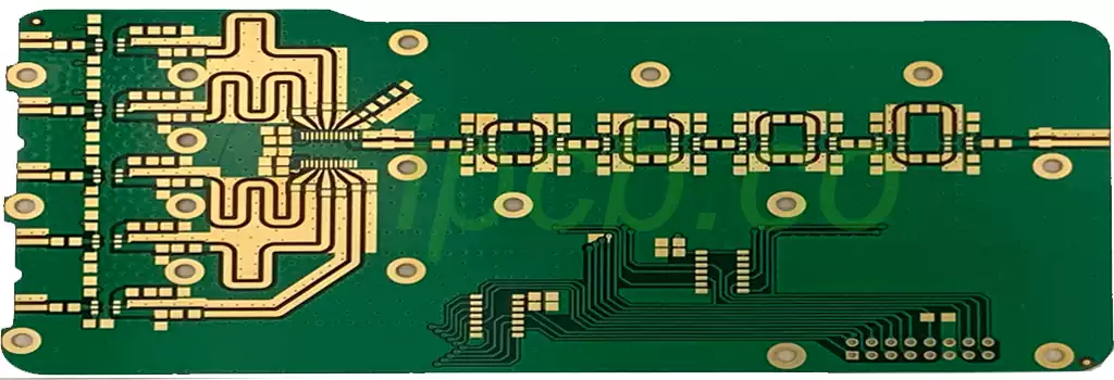
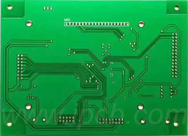
The PCB layout file is the physical realization of the schematic. Once the electrical design has been verified and the circuit functions as intended, PCB designers transform the schematic into a physical board layout. The layout file contains all manufacturing-related information, including the board outline, component placement, copper routing, vias, mounting holes, and every other physical feature required for PCB fabrication and assembly.
Unlike the schematic, which focuses on electrical theory, the PCB layout directly determines the board’s electrical performance and manufacturability. Engineers use the layout file to build prototype PCBs and evaluate key performance factors such as circuit functionality, thermal performance, current-carrying capacity, and overall reliability. After the prototype successfully passes all verification tests, the finalized design files are released for volume production.
Key Characteristics of a PCB Schematic
1.Components are not drawn to scale.
To clearly illustrate electrical connections, components and wires in a schematic are intentionally simplified and are not drawn according to their actual physical dimensions or spacing. Components that are physically adjacent on the finished PCB may appear far apart in the schematic to improve readability.
2.Signal lines may cross without indicating physical routing.
Electrical connections in a schematic are allowed to cross each other because the purpose is to represent logical connectivity rather than physical routing. These crossing lines do not imply that traces will intersect on the actual PCB. Connections between different PCB layers are represented using standardized net labels, connectors, or cross-reference symbols rather than physical routing paths.
3.Schematics support multiple pages and functional hierarchy.
Simple circuits may be documented on a single schematic page, while complex electronic systems are typically divided into multiple pages or organized into hierarchical functional blocks. This modular organization improves readability and simplifies circuit analysis. However, the functional grouping shown in the schematic does not necessarily correspond to the physical placement of components on the finished PCB.

Key Characteristics and Design Considerations of a PCB Layout File
A PCB layout file represents the actual physical design of the circuit board. It supports single-layer, double-layer, and multilayer PCB designs, with double-layer PCBs being among the most widely used in consumer electronics. Every component, copper trace, via, and mounting hole is positioned according to its exact physical dimensions and manufacturing requirements, ensuring the design can be fabricated accurately.
During PCB layout, engineers must consider both electrical performance and manufacturing constraints to ensure reliable operation. Proper spacing between components should be maintained to provide sufficient heat dissipation and prevent thermal accumulation during operation. Connectors and edge interfaces must be positioned correctly to accommodate the overall mechanical assembly of the product. Copper trace widths and copper thickness should be designed according to current-carrying requirements and thermal performance to ensure adequate power delivery and heat management.
The PCB layout file also includes a dedicated silkscreen layer, which identifies component reference designators, polarity markings, pin numbers, and other assembly information using text and graphical symbols. These markings facilitate PCB assembly, inspection, troubleshooting, and maintenance.
After the PCB layout is completed, the design must undergo prototype assembly and functional testing to verify that every component operates according to the intended design specifications. If functional problems or performance deficiencies are identified, the physical layout must be revised and optimized before the design is approved for production.
The PCB schematic and the PCB layout file are two independent but closely connected stages of the PCB development process. Both are indispensable. The schematic provides the theoretical foundation by defining the circuit’s electrical connectivity and functional behavior, while the PCB layout transforms that electrical design into a manufacturable physical board. The quality of the PCB layout directly influences electrical performance, mechanical integrity, manufacturability, and the long-term reliability of the finished product.