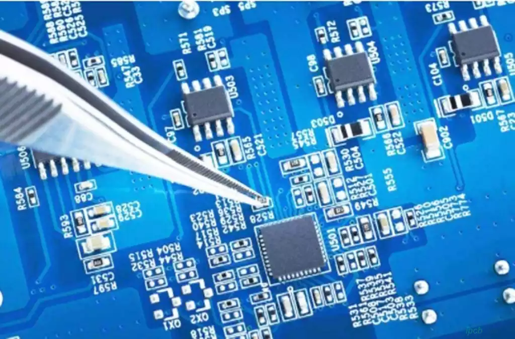
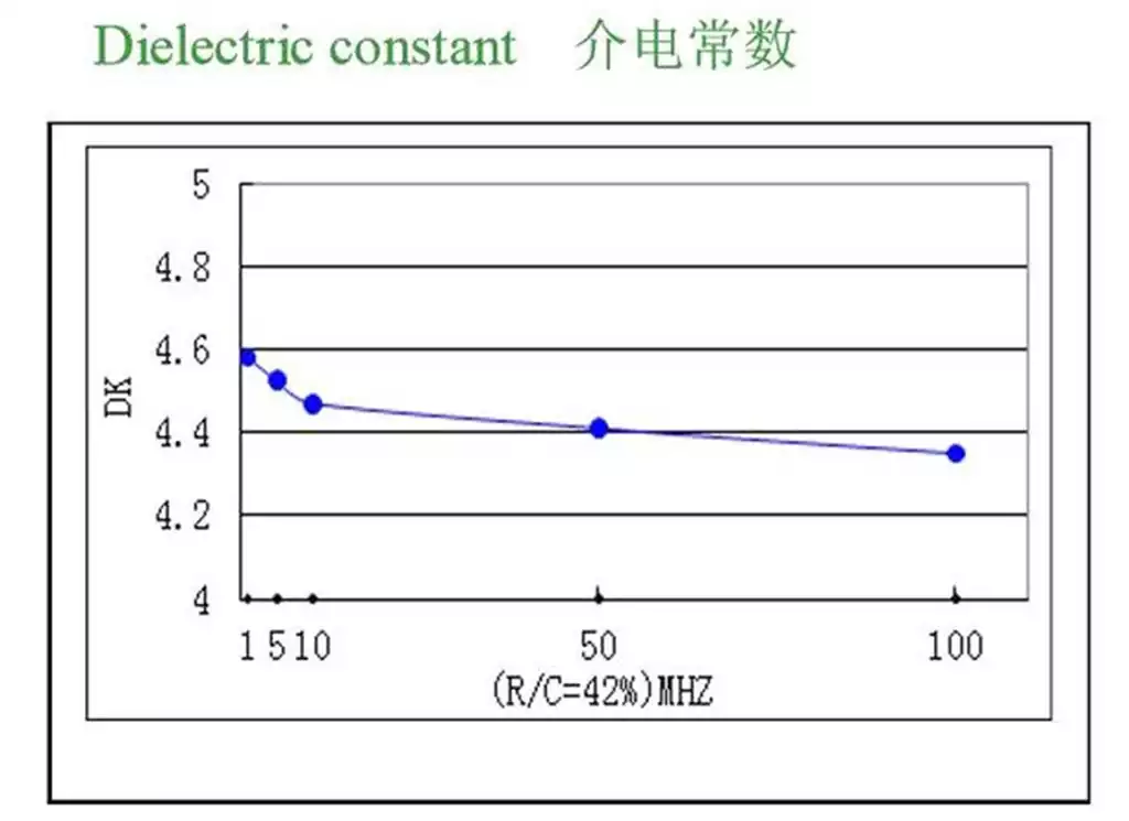
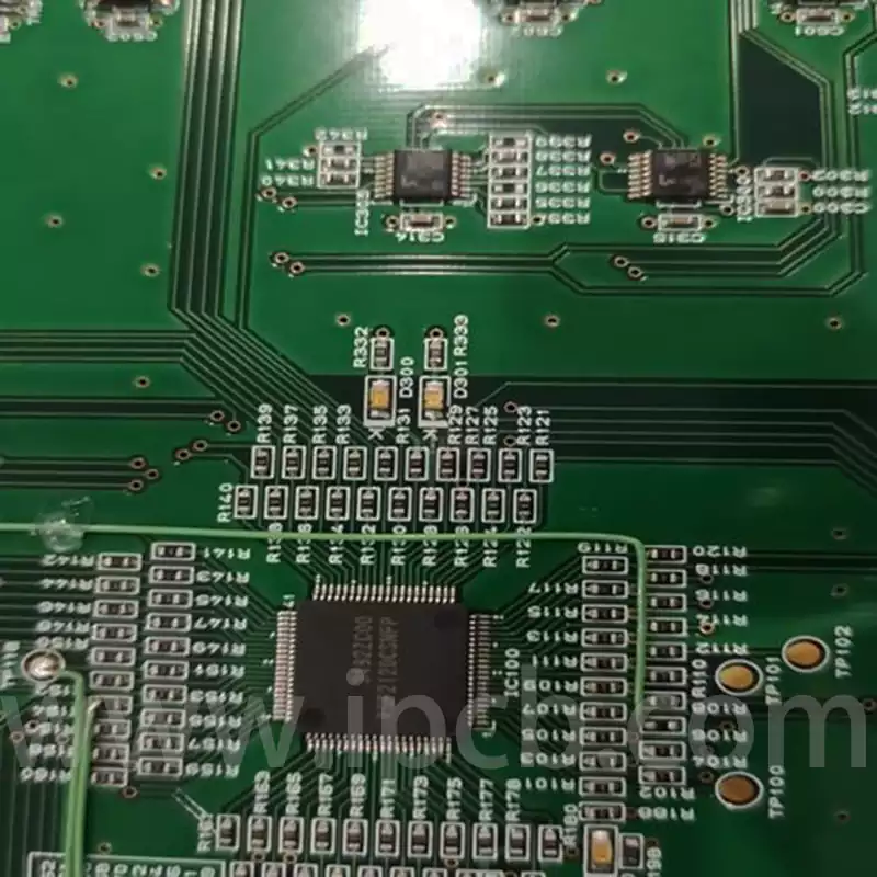
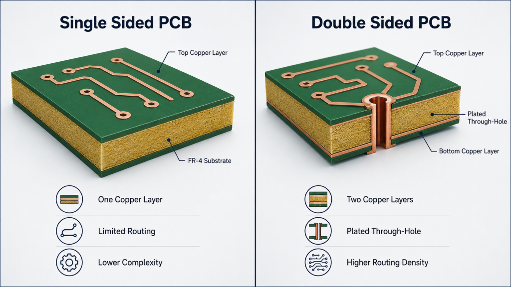
A cutaway view of a double sided copper clad PCB board, showing the copper layers, FR-4 core and plated through-hole interconnection.
A double sided copper clad PCB board may appear to be one of the simplest structures in printed circuit manufacturing: a dielectric core covered by copper foil on both surfaces. However, its electrical behaviour and long-term reliability depend on a complex interaction between copper geometry, resin chemistry, glass-fibre reinforcement, drilled-hole quality and electroplated copper.
The defining engineering challenge is not merely producing two circuit patterns. It is creating a mechanically and electrically stable three-dimensional connection through a material system whose constituents expand, deform and conduct heat in very different ways.
Before processing, the material is more precisely described as a double-sided copper-clad laminate. It becomes a printed circuit board only after the copper layers have been patterned and electrically interconnected. This distinction matters because many performance limitations originate in the laminate and copper foil before the first circuit image is transferred.
How a Double Sided Copper Clad PCB Board Works
The Material Interface Beneath the Copper
The central core of a conventional double sided copper clad PCB board is usually FR-4, a composite consisting of woven glass fabric impregnated with flame-retardant epoxy resin. The glass fibres provide dimensional stability and mechanical strength, while the cured resin fills the spaces between the fibres and provides electrical insulation.
Copper foil is bonded to both surfaces during laminate production. Although the finished interface appears flat macroscopically, its microscopic structure is deliberately irregular. The bonding surface of electrodeposited copper is treated to create a controlled roughness that allows the resin to anchor mechanically to the foil.
This roughness improves peel strength, but it also introduces an electrical trade-off. At low frequencies, current flows through most of the conductor cross-section. As frequency rises, the skin effect increasingly concentrates current near the copper surface.
The approximate skin depth is given by: delta = square root of (2 times rho divided by (omega times mu)), where rho is copper resistivity, omega is angular frequency and mu is magnetic permeability.
When the skin depth becomes comparable to the copper surface profile, the current must follow a longer microscopic path. This increases effective AC resistance and conductor loss. Very-low-profile or reverse-treated copper foil may therefore be selected for fast digital, RF or controlled-impedance designs.
For most low-frequency double-sided boards, this effect is relatively small. It becomes significant when the same two-layer structure carries high-frequency signals or digital signals with fast rise and fall times. In such applications, copper roughness becomes part of the signal-integrity model rather than merely a laminate-manufacturing detail.
Why Two Copper Layers Change the Electrical Structure
A single-sided PCB confines every conductor to one copper surface. Once copper is introduced on both sides, the board begins to behave as a coupled electromagnetic structure.
A signal trace on the top surface does not operate independently of the copper beneath it. If the bottom surface contains a continuous ground region, the signal current produces a corresponding return current in that ground conductor. At higher frequencies, the return current concentrates beneath the signal path because this produces the lowest-inductance return loop.
The dielectric thickness, copper thickness and relative permittivity consequently influence the characteristic impedance of the trace. A top-layer conductor referenced to bottom-layer ground behaves approximately as a microstrip, although glass weave, solder mask and interruptions in the ground copper make the real structure more complicated.
A two-layer board rarely provides the same field confinement as a multilayer PCB with dedicated reference planes. Routing on the lower layer can divide the ground region into disconnected areas, forcing return current to travel around slots and interruptions. The resulting increase in loop area raises inductance and can worsen radiated emissions, crosstalk and ground bounce.
An effective two-layer design is therefore not simply a single-sided layout distributed across two surfaces. The two copper layers must be treated as an interacting signal-and-return system.
Short signal paths, continuous return regions and deliberate ground-via placement usually produce greater electrical improvement than adding copper without considering how current returns to its source.
How the Two Copper Layers Are Connected
The Plated Through Hole as a Three-Dimensional Conductor
The most important structural feature of a double-sided PCB is the plated through hole. Without hole-wall metallisation, the upper and lower copper patterns remain physically separated by the insulating core.
Mechanical drilling initially creates a non-conductive cylindrical wall containing exposed glass fibres and cured resin. Drilling also generates heat. If drill geometry, feed rate or tool condition is poorly controlled, softened resin can smear across the hole wall and cover exposed copper near the layer interfaces.
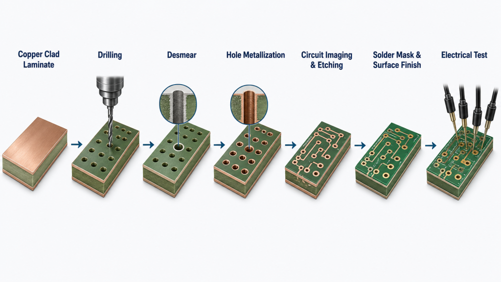
This residue must be removed before metallisation. The desmear process cleans and modifies the hole wall, exposing a surface that can be conditioned for chemical copper deposition.
A thin electroless copper layer is then deposited over the resin, glass fibres and exposed copper. This deposit does not provide the complete current-carrying thickness. Its primary purpose is to establish a continuous conductive seed layer over the previously non-conductive hole wall.
Electrolytic copper plating subsequently builds the required copper thickness inside the hole and usually increases the copper thickness on the external surfaces.
Manufacturing sequence from laminate drilling and hole metallisation to circuit formation, surface finishing and electrical testing.
The finished hole is not a solid copper tube inserted into the laminate. It is a relatively thin electroplated copper cylinder bonded to a composite wall of resin and glass fibre. Its reliability depends on plating continuity, copper ductility, thickness distribution, drilling quality and laminate expansion.
Small holes in thick boards are especially demanding. As the ratio between board thickness and finished hole diameter increases, solution exchange and electrical current distribution inside the hole become less uniform. Copper may build more rapidly near the hole entrances than at the centre of the barrel.
A plated hole can consequently appear satisfactory at the surface while containing insufficient copper near its middle. Cross-section inspection is used to reveal this hidden thickness distribution and evaluate the quality of the hole wall, copper deposit and layer connections.
Thermal Expansion and Barrel Fatigue
Copper and FR-4 do not expand at the same rate. Within the plane of the board, woven glass reinforcement restricts laminate movement. Through the board thickness, however, the resin-rich structure expands more strongly as temperature rises, especially when the resin system passes its glass transition temperature.
The copper barrel is bonded to this expanding material. During soldering, reflow and repeated operating-temperature cycles, the laminate stretches the barrel in the Z-axis. When the board cools, the structure contracts again.
A sufficiently thick and ductile copper deposit can tolerate this cyclic strain. A barrel containing thin regions, inclusions or microcracks is less able to deform without damage. Repeated expansion may eventually initiate a circumferential crack in the plated copper.
This type of defect can be difficult to diagnose because the connection may remain continuous at room temperature and open only when the board is heated or mechanically stressed.
The glass transition temperature, commonly called Tg, is relevant, but Tg alone does not determine reliability. Z-axis coefficient of thermal expansion, decomposition temperature, moisture absorption and time above Tg also influence the strain applied to the plated hole.
A high-Tg laminate cannot compensate for poor drilling, inadequate desmearing or insufficient hole-wall copper. Reliability emerges from the complete material and manufacturing system.
How Copper Geometry Affects Manufacturability
Copper Thickness Is Not Only a Current Rating
Copper weight is often treated as a current-capacity specification. One-ounce copper, with a nominal starting thickness of approximately 35 micrometres, is widely used in general electronic products.
Increasing copper thickness enlarges the conductor cross-section and reduces DC resistance. The resistance R equals rho times L divided by (w times t), where L is conductor length, w is conductor width and t is copper thickness.
The power converted into heat is P = I squared times R.
Thicker copper can therefore reduce conductor loss for a given trace geometry. However, the temperature of a finished conductor cannot be predicted from copper thickness alone. Heat must spread through the copper pattern, cross the dielectric and leave the assembly through conduction, convection or an external thermal structure.
Copper geometry can be as important as nominal copper weight. A wide copper region connected through a narrow neck remains limited by the neck. Similarly, a thermal pad connected to the opposite surface by too few vias may retain heat near the component even when large copper pours are present.
Copper thickness also changes manufacturing capability. During etching, copper is removed vertically through its thickness and laterally beneath the resist edge. This lateral component creates undercut and reduces the final conductor width.
Because thicker copper requires a longer vertical etching path, the etchant has more time to attack the trace sidewalls. Heavy copper therefore generally requires wider conductors and larger spaces than standard copper.
Attempting to combine thick copper with very fine geometry can produce trapezoidal traces, excessive width loss and unstable conductor spacing. The production artwork must include an etching allowance based on copper thickness, chemistry, equipment and process behaviour.
This allowance is a controlled manufacturing correction. It is not an arbitrary enlargement of every circuit feature.
Pattern Registration and Annular-Ring Integrity
Drilled holes and circuit images are produced in separate manufacturing stages. Their positions can never coincide with mathematical perfection.
Drill runout, laminate movement, imaging tolerance and etching variation all contribute to positional error. The annular ring surrounding a plated hole provides the geometric margin needed to absorb these tolerances.
When the annular ring is too narrow, even a small displacement can move the drilled hole close to the pad edge or cause a breakout. A breakout does not always create an immediate open circuit because part of the plated barrel may remain connected to the conductor. It nevertheless reduces mechanical and electrical margin.
Registration must be considered on both sides simultaneously. A hole that appears centred on the top pad may be offset on the bottom because the two circuit images are not perfectly aligned with each other or with the drilled panel.
Aggressive pad reduction should therefore not be used merely to create more routing space. The apparent gain in layout density may be offset by lower fabrication yield and weaker plated-hole connections.
Copper Balance and Board Flatness
Copper has different stiffness and thermal behaviour from the underlying laminate. If one side of a double-sided board contains a nearly continuous copper area while the opposite side contains only sparse traces, the structure becomes mechanically unbalanced.
During solder mask curing, surface finishing and assembly, thermal exposure causes the two sides to respond differently. The resulting residual stress may appear as bow or twist.
Copper balance does not require identical circuit patterns. It means avoiding unnecessarily extreme differences in copper coverage and maintaining reasonable structural symmetry across the board and production panel.
Non-functional copper may be introduced to improve plating uniformity and dimensional balance, but it must be added with electrical intent. Random copper filling can change parasitic capacitance, interfere with antenna structures or create floating conductive islands.
Copper balancing is therefore both a mechanical and an electromagnetic design decision.
Additional Material and Assembly Risks
Moisture, Soldering Heat and Delamination
Epoxy laminates absorb a limited amount of moisture from their environment. During rapid heating, absorbed moisture expands and can generate local vapour pressure within resin-rich regions or at weak material interfaces.
If storage and pre-baking controls are inadequate, soldering heat may produce blistering, measling or delamination. The risk increases when the laminate has been stored in humid conditions, subjected to multiple soldering cycles or processed close to its thermal limit.
The copper-to-laminate bond is particularly vulnerable around narrow pads and conductors. During manual rework, excessive temperature or prolonged contact can soften the resin system and weaken adhesion. Pulling a component lead before the solder is completely molten may then lift the pad from the substrate.
High peel strength improves resistance to this failure, but process control remains essential. Even a qualified laminate can be damaged by uncontrolled soldering or rework.
Surface Finish as an Extension of the Copper System
After etching and solder mask application, exposed copper pads require protection. Bare copper oxidises rapidly, and the oxide layer interferes with solder wetting and contact reliability.
Surface finish does not change the internal two-layer structure, but it determines how exposed pads resist oxidation and interact with the assembly process. HASL is economical for conventional components, while the flatter surfaces produced by ENIG and OSP are more compatible with fine-pitch assembly.
ENIG introduces a nickel diffusion barrier between the copper and the thin immersion-gold layer. OSP instead protects the copper with a thin organic film and avoids adding a metallic layer to the pad. Each process has different requirements for handling, storage, thermal exposure and soldering.
The correct finish should be selected according to pad geometry, assembly process, storage period, contact requirements and expected rework, not by appearance alone.
When a Two-Layer PCB Is No Longer Enough
A double-sided copper-clad PCB is effective when routing density remains moderate and signal return paths can be preserved. It provides more routing freedom than a single-sided board without introducing the lamination complexity of a multilayer PCB.
Its limitations become apparent when the design requires uninterrupted ground references, multiple controlled power domains, dense BGA escape routing or numerous high-speed interfaces.
Attempting to force these connections onto two layers can produce fragmented ground copper, long return paths, excessive via usage and difficult electromagnetic compatibility behaviour.
Moving to a four-layer structure is not simply a way to obtain two additional routing surfaces. Dedicated internal reference planes fundamentally change electromagnetic behaviour by reducing loop inductance, improving field confinement and providing more predictable impedance.
The correct layer count is determined by circuit physics rather than component count alone. A carefully designed two-layer PCB can outperform a poorly designed multilayer board, but it cannot reproduce all the structural advantages of continuous internal planes.
The Real Engineering Value of a Double Sided PCB
The apparent simplicity of a double-sided PCB conceals a precise three-dimensional manufacturing system. The external copper patterns must maintain controlled geometry, the plated barrels must survive repeated Z-axis expansion, and the laminate must preserve adhesion and insulation through drilling, chemical processing and soldering.
Board quality cannot be judged solely by whether the initial electrical test passes. A board may pass continuity testing while containing marginal annular rings, thin barrel copper, resin smear or excessive thermal stress. These weaknesses often become visible only after assembly or field operation.
Reliable production therefore depends on linking design rules to real manufacturing capability. Copper thickness must correspond to achievable etching geometry. Hole diameter must remain compatible with board thickness and plating distribution. Material properties must match the assembly temperature and operating environment. Copper coverage must support both electrical performance and structural balance.
iPCB provides double-sided PCB manufacturing from prototype verification to volume production. Through engineering review of laminate selection, hole structure, copper distribution, conductor geometry and surface finish, potential manufacturability and reliability risks can be identified before fabrication.
A double sided copper clad PCB board is not simply copper bonded to both sides of an insulating sheet. It is a coupled electrical, thermal and mechanical structure, and its performance depends on how accurately those three domains are engineered together.