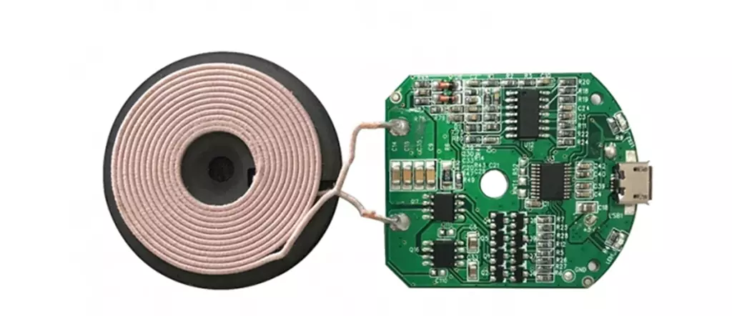
A printed circuit board soldermask is a special construction designed to protect the integrity and stability of a circuit board by preventing solder from penetrating into areas of the board that should not be soldered during the soldering process.
Soldermasks are typically placed on the substrate of a circuit board to cover a predetermined portion of the circuit layout. In the soldermask layer, microscopic holes are created to expose the wires located underneath these holes. The solder pad layer then has an inner layer (e.g., a copper foil layer) and an outer layer (e.g., a nickel-gold layer), wherein the inner layer is adhered to the sidewalls of the microvias and electrically connected to the exposed wires, and the outer layer is adhered to the inner layer to form a solder pad.
Its main function is to protect the integrity and stability of the board by preventing solder from penetrating into areas of the board that should not be soldered during the soldering process. During the soldering process, solder is highly mobile, and without effective anti-soldering measures, solder is likely to penetrate into tiny gaps or areas of the board that should not be soldered, resulting in short circuits or performance degradation. Through its unique material and structural design, solder protection pads can effectively stop the penetration of solder and ensure the soldering quality and stability of circuit boards.
When choosing a protective pad, you need to consider several key factors:
First, the material is crucial. The pads should be made of a well-insulating material, such as rubber, silicone or plastic. This ensures that the pads meet the specific needs of the board’s soldering surface, effectively preventing short circuits or other potential risks during the soldering process.
Secondly, size is also a factor that should not be overlooked. The size of the pad should match the surface you are working on, both to ensure that there is enough space for you to freely solder the board and to avoid the pad wobbling or shifting while you are working on it.
Finally, the thickness needs to be carefully considered. The thickness of the pads should be moderate to ensure that the boards are adequately protected from damage. Generally speaking, a rubber protective mat that is about 1/4 inch thick will provide adequate protection.
When using protective pads, you need to follow these key steps and considerations:
First, accurate placement of the protective mat is critical. Make sure the pad is placed under the surface to be protected and facing the table. When you are soldering, the board should be securely placed on the pad and avoided as much movement as possible to ensure that the pad is effective in its protective role.
Secondly, it is also important to keep the pad clean. Before using the pads, you should clean the work surface to remove dust, debris, and other debris that could interfere with soldering. This ensures quality soldering and prevents damage to the board structure. If there is dirt or residue on the surface of the protective pad, you can wipe it down with alcohol or another appropriate cleaning solution to keep it clean and effective.
Finally, it is necessary to replace the protective pads periodically. Protective mats may wear out or become damaged after prolonged use, so their condition needs to be checked regularly. If you see signs of wear or damage to the pads, you should replace them with new ones immediately to ensure their continued effectiveness in protecting the board.
The soldermask in a circuit board is one of the key elements in safeguarding the quality and stability of the board. By gaining a deeper understanding of their function and use, we can better utilize it to improve the manufacturing quality and usability of circuit boards.