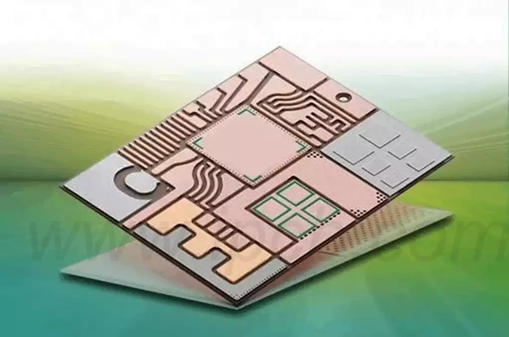
SMD package refers to electronic components directly surface mounted on the circuit board in a package, it has a small size, light weight, high reliability, is currently the most widely used in electronic products in a package.
SMD surface mount device installation process mainly has the following steps:
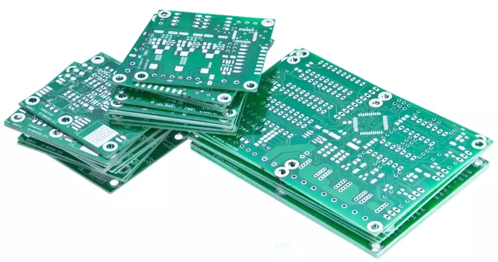
Installation of the substrate: the substrate will be fixed on the countertop
Point paste or glue: according to the size of the components, the SMD adhesive coated in a pre-determined position, if the assembly process using reflow soldering, it is necessary to apply the paste in the substrate pads, the current commonly used medium – high temperature level Sn-Ag solder paste.
Installation of SMD: Generally use automated professional mounter, mainly including: pick and place the SMD suction and loading head, X-Y working table, program control system and feeding part.
Thermal curing: carried out after the dispensing and placement of SMD, the adhesive is cured by curing oven under certain temperature and time control. The curing process is carried out in a curing oven under a certain temperature and time control to improve the adhesive strength of the SMD, and to prevent the components from being shifted due to vibration and impact during storage and transportation.
SMD soldering: using SMD adhesive bonded wave soldering and solder paste bonded reflow soldering two ways.
Cleaning: Remove residual adhesive to prevent corrosion of the substrate.
Inspection and testing: Solderability is checked according to standards and test requirements.
Common SMD package sizes
1.0201 package: size 0.6 * 0.3mm, suitable for high-density PCB boards, with excellent high-frequency characteristics, but lower voltage.
2.0402 package: size 1.0 * 0.5mm, suitable for general circuit board, pressure and heat resistance is better.
3.0603 package: size 1.6 * 0.8mm, suitable for medium density printed circuit board, pressure and heat resistance is excellent.
4.0805 package: size 2.0 * 1.25mm, for low-density PCB substrate, pressure and heat resistance is good.
5.1206 package: size 3.21.6mm, suitable for general circuit board, good pressure and heat resistance. 6.1210 package: size 3.22.5mm, suitable for high power circuits and industrial areas.
7.2010 package: size 5.0*2.5mm, suitable for high power circuits and industrial areas.
8.2512 package: size of 6.4 * 3.2mm, suitable for high-power circuits and industrial areas, the best pressure and heat resistance.
In the SMD package method, the pins of the components are directly connected to the PCB (Printed Circuit Board) by soldering or pasting without inserting into the holes. One of the main advantages of this type of package is that it can greatly reduce the spacing between components, thus making the entire board more compact and space-saving. This is essential for today’s increasingly compact electronic product designs.
In addition, SMD packaging can also improve the performance and reliability of the board. Since the pins of SMD components are directly connected to the PCB, the connection length between the pins is reduced, thus reducing the resistance and inductance of the circuit and improving the stability of signal transmission. In addition, the SMD packaging method can also reduce the number of welding points, reduce the impact of welding quality on the entire circuit, and improve the reliability of the circuit.
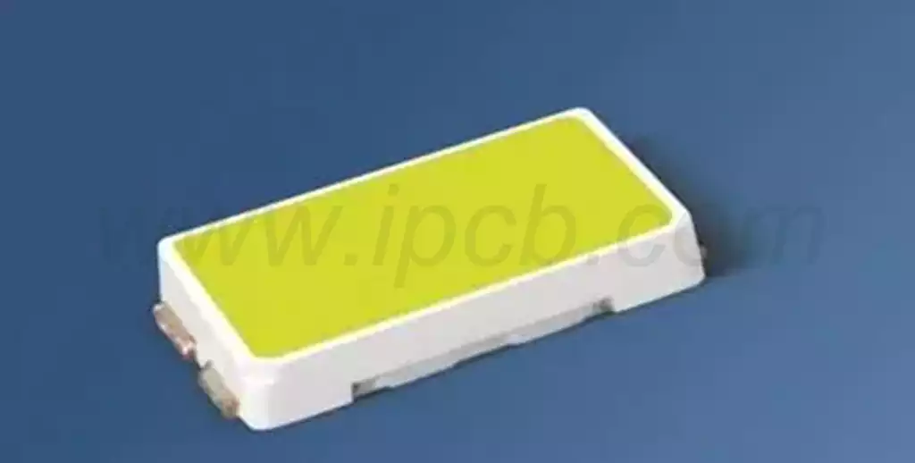
In practical applications, SMD packaging method has a wide range of components, including chip resistors, chip capacitors, chip inductors, SMD diodes, SMD transistors and so on. These components are widely used in a variety of electronic devices, such as cell phones, tablet PCs, televisions, medical devices, and so on. Since the SMD package method has the advantages of small size, light weight, high efficiency, etc., it is widely used in these electronic products.
Surface Mount Discrete Resistors (SMD Resistors)
There are two main types of surface mount resistors: thick film and thin film.
Thick film surface mount resistors are made by screening a resistive film (ruthenium dioxide based paste or similar) on the surface of a flat, high purity alumina substrate, rather than depositing a resistive film on a round core as is done for axial resistors. The resistance value is obtained by changing the composition of the resistive paste before screening and by laser trimming the film after screening.
In thin film resistors, the resistive element sits on a ceramic substrate with a protective layer on top (glass passivation) and solderable terminals on the sides (tin-lead). The terminals have an adhesion layer on the ceramic substrate (silver deposited as a thick film paste), followed by a nickel barrier backing layer, followed by an impregnated or electroplated solder coating. The nickel barrier layer is important to maintain the solderability of the terminals because it prevents the silver or gold electrodes from leaching (dissolving) during the SMD soldering process.
Resistors are available in 1/16, 1/10, 1/8, and ¼ watt ratings, with resistance values ranging from 1 ohm to 100 megohms, and in a variety of sizes and tolerances. Common sizes are 0402, 0603, 0805, 1206, and 1210. surface mount resistors have a colored resistive layer with a protective coating on one side, and usually a white base material on the other. Therefore, resistors and capacitors can be simply distinguished from each other by their appearance.
Ceramic Capacitors for SMT
Surface mount capacitors are ideal for high frequency circuit applications because they do not have any leads and can be placed underneath the package on the other side of the PCB assembly. The most widely used package for ceramic capacitors is the 8mm tape and reel package.
Surface mount capacitors can be used for decoupling applications and frequency control. Multilayer monolithic ceramic capacitors are more volume efficient. They are available in different dielectric types according to EIA RS-198n, i.e. COG or NPO, X7R, Z5U and Y5V.
Surface mount capacitors are highly reliable and have been used in large numbers in automotive under hood applications, military equipment and aerospace applications.
Surface Mount Tantalum Capacitors
For surface mount capacitors, the dielectric can be ceramic or tantalum.
Surface mount tantalum capacitors have very high volumetric efficiency or high capacitance-voltage product per unit volume and high reliability.
Lower-lead wrap-around capacitors, often referred to as plastic molded tantalum capacitors, have leads instead of terminals and a beveled top as a polarity indicator. There are no soldering or placement considerations when using molded tantalum capacitors. They are available in two case sizes – standard and extended.
Tantalum capacitors in different case sizes have capacitance values from 0.1 to 100µF and DC voltages from 4 to 50V. They can also be customized according to application requirements. Tantalum capacitors are available in bulk, waffle packs and tape and reel with or without marked capacitance values.
Tubular Passive SMD Components for SMT
Cylindrical devices known as metal electrode leadless faces (MELF) are used for resistors, jumpers, ceramic and tantalum capacitors, and diodes. They are cylindrical and have metal end caps for soldering.
Because MELFs are cylindrical, there is no need to place the resistive element away from the surface of the board, as is the case with rectangular resistors.MELFs are less costly. As with conventional axial devices, MELF values are color coded.MELF diodes are identified as MLL41 and MLL34.MELF resistors are identified as 0805, 1206, 1406, and 2309.
SMD packaging technology, with its miniaturization, high density and high performance, is leading electronics into a more compact and powerful future.